TOTAL- ACEXTREME® SIGNALS
Data Device Corporation DS-BU-67301B-G
www.ddc-web.com
1/14
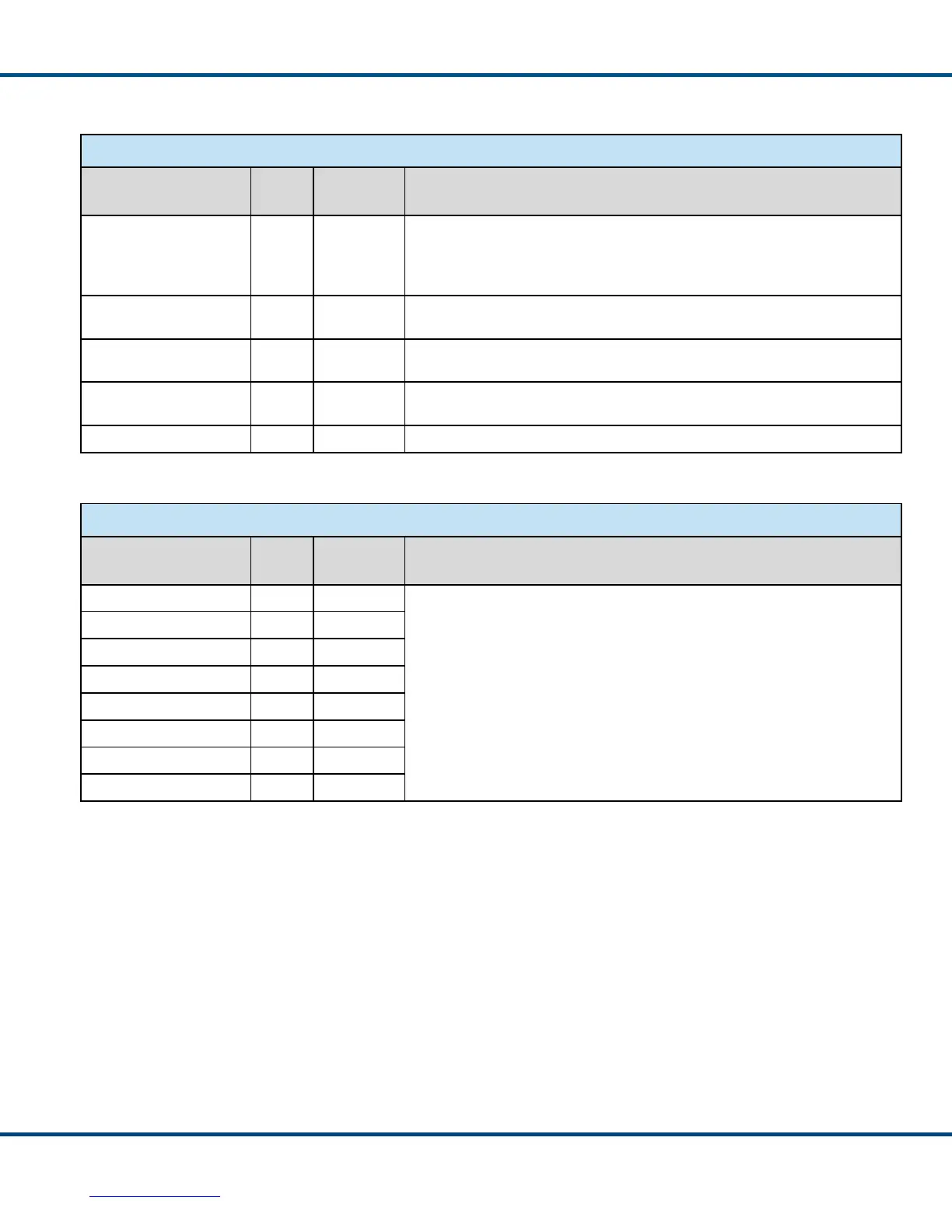
Table 16. JTAG Test
Signal Name BALL Pullup/
Pulldown
Description
JTAG_TCK (I) A7 50k Pullup This ball is the JTAG test clock.
The Test Clock is used to load the test mode data from the JTAG TMS pin,
and the test data on the TDI pin [on the rising edge]. On the falling edge test
clock outputs the test data on the TDO pin.
JTAG_TMS (I) A10 50k Pullup This ball is the test mode select input signal. Controls the operation of the
test logic, by receiving the incoming data.
JTAG_TDI (I) B10 50k Pullup This ball is the serial test data input. Receives serial input data which is either
fed to the test data registers or instruction register.
JTAG_TDO (O) B8 N/A This ball is the serial test data output. Outputs serial data which comes from
either the test data registers or instruction register.
JTAG_nTRST (I) B9 50k Pullup This ball is test reset and will asynchronously reset the JTAG test logic.
Table 17. General Purpose Discrete I/O
Signal Name BALL Pullup/
Pulldown
Description
DISCRETE_IO_7 (I/O) H12 50k Pullup Discrete I/O (Digital Logic levels)
Following power-up, each register is reset to zero, and all outputs are reset to
high impedance state (input mode). All registers are read/write. Each
Discrete IO bit is independently programmable for input vs. output, and each
bit has independent 3-state control.
DISCRETE_IO_6 (I/O) L14 50k Pullup
DISCRETE_IO_5 (I/O) J12 50k Pullup
DISCRETE_IO_4 (I/O) J13 50k Pullup
DISCRETE_IO_3 (I/O) L13 50k Pullup
DISCRETE_IO_2 (I/O) K12 50k Pullup
DISCRETE_IO_1 (I/O) K13 50k Pullup
DISCRETE_IO_0 (I/O) M14 50k Pullup
 Loading...