TOTAL- ACEXTREME® SIGNALS
Data Device Corporation DS-BU-67301B-G
www.ddc-web.com
1/14
11.2 Host Interface Signals
11.2.1 PCI Signals
Note that most of these signals are dual use. That is, they take on different function,
depending on whether the Total-AceXtreme® is configured for PCI mode or for
FGPI mode.
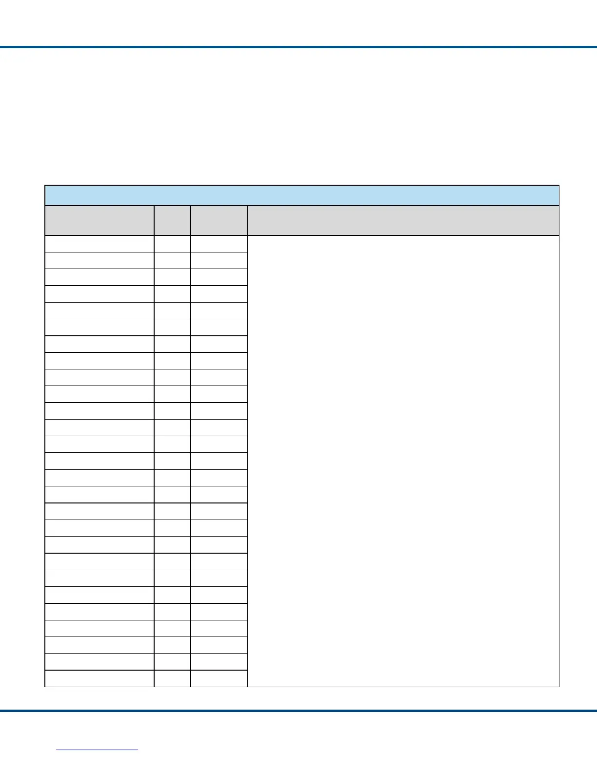
Table 18. PCI Signals
Signal Name BALL Pullup/
Pulldown
Description
PCI_AD(31) (I/O) MSB A5 None
32-Bit PCI Bus Address / Data lines. Address and Data are multiplexed on
the same pins. Each bus operation consists of an address phase followed by
one or more data phases.
Address phases are identified when the control signal FRAME# is asserted.
Data transfers occur during those clock cycles in which the control signals
IRDY# and TRDY# are both asserted.
PCI_AD(30) (I/O) A4 None
PCI_AD(29) (I/O) B5 None
PCI_AD(28) (I/O) B4 None
PCI_AD(27) (I/O) B3 None
PCI_AD(26) (I/O) D1 None
PCI_AD(25) (I/O) C2 None
PCI_AD(24) (I/O) D3 None
PCI_AD(23) (I/O) F1 None
PCI_AD(22) (I/O) E2 None
PCI_AD(21) (I/O) E3 None
PCI_AD(20) (I/O) F3 None
PCI_AD(19) (I/O) G1 None
PCI_AD(18) (I/O) G3 None
PCI_AD(17) (I/O) J5 None
PCI_AD(16) (I/O) H1 None
PCI_AD(15) (I/O) K1 None
PCI_AD(14) (I/O) M2 None
PCI_AD(13) (I/O) L1 None
PCI_AD(12) (I/O) N1 None
PCI_AD(11) (I/O) L3 None
PCI_AD(10) (I/O) K2 None
PCI_AD(09) (I/O) M1 None
PCI_AD(08) (I/O) N2 None
PCI_AD(07) (I/O) N3 None
PCI_AD(06) (I/O) N4 None
PCI_AD(05) (I/O) M4 None
 Loading...