Data Device Corporation 97 DS-BU-67301B-G
www.ddc-web.com
1/14
7 POWER INPUTS
7.1 Decoupling Capacitors
For the Total-AceXtreme’s power supply input, DDC recommends the use of the
following decoupling capacitors:
• For +1.8V_CORE (7 balls):
o 1 - 0.1uF Ceramic Chip
o 1 - 0.01uF Ceramic Chip.
• For +3.3V_LOGIC (12 balls):
o 1 - 10uF Ceramic Chip or 10uF Low ESR/ESL Tantalum
o 3 - 0.1uF Ceramic Chip
o 8 - 0.01uF Ceramic Chip
• For +3.3V_XCVR (11 balls):
o 2 - 10uF Ceramic Chip or 10uF Low ESR/ESL Tantalum
o 2 - 0.1uF Ceramic Chip
o 6 - 0.01uF Ceramic Chip
• For +1.8V_PLL (1 ball):
o 1 - 0.1uF Ceramic Chip
o 1 - 0.01uF Ceramic Chip
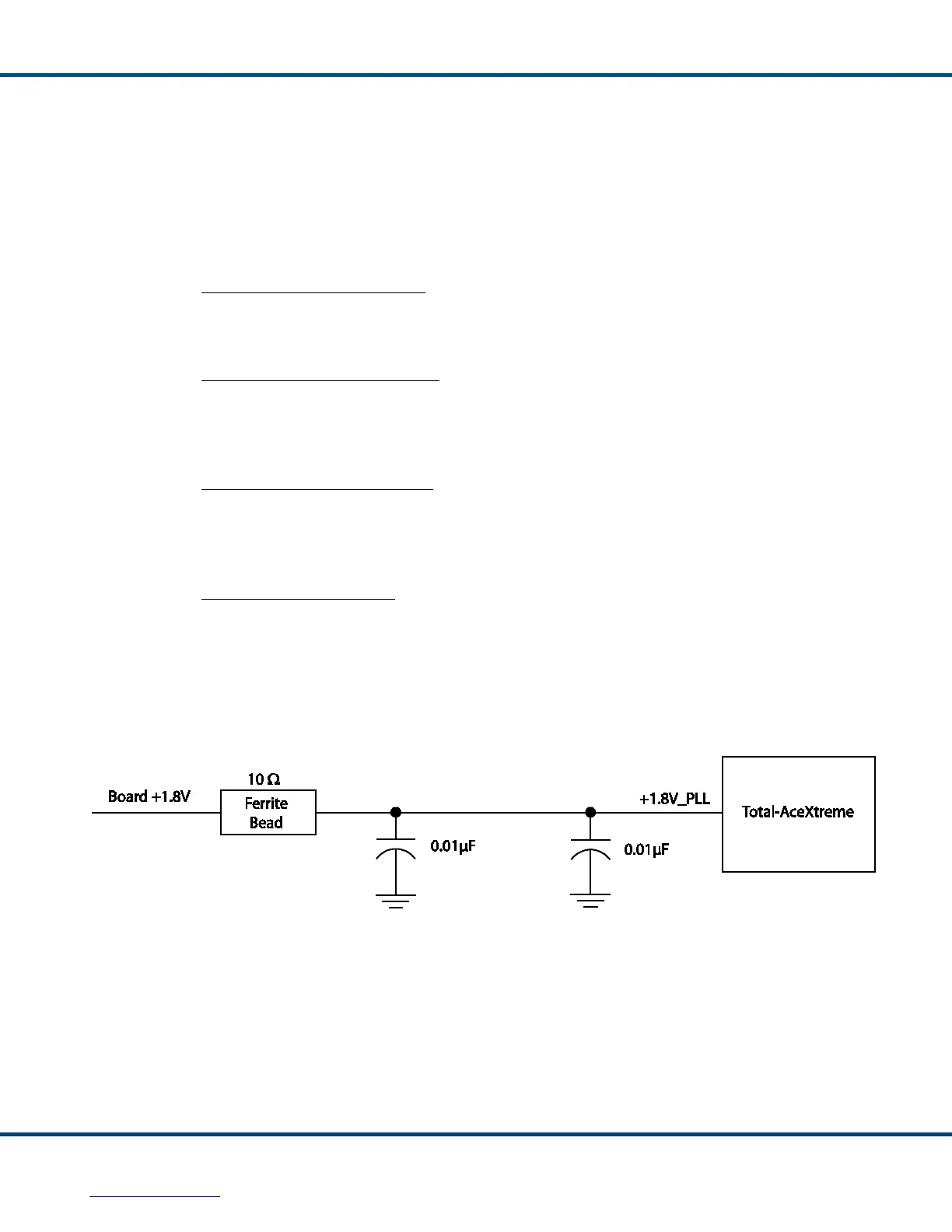
In order to minimize power supply noise on the PLL supply pin, DDC recommends
the use of a ferrite bead in series with decoupling capacitors as shown in Figure 55.
Figure 55. Recommended +1.8V_PLL Filter Network
7.2 Power Sequencing
In order to ensure proper initialization of the Total-AceXtreme under all conditions, it
is necessary to perform the power-up initialization sequence described below. Figure
56 illustrates the required timing relationships for the Total-AceXtreme’s power
inputs, the CLK_IN and nPOR input signals, and the PLL_LOCKED output signal.
 Loading...