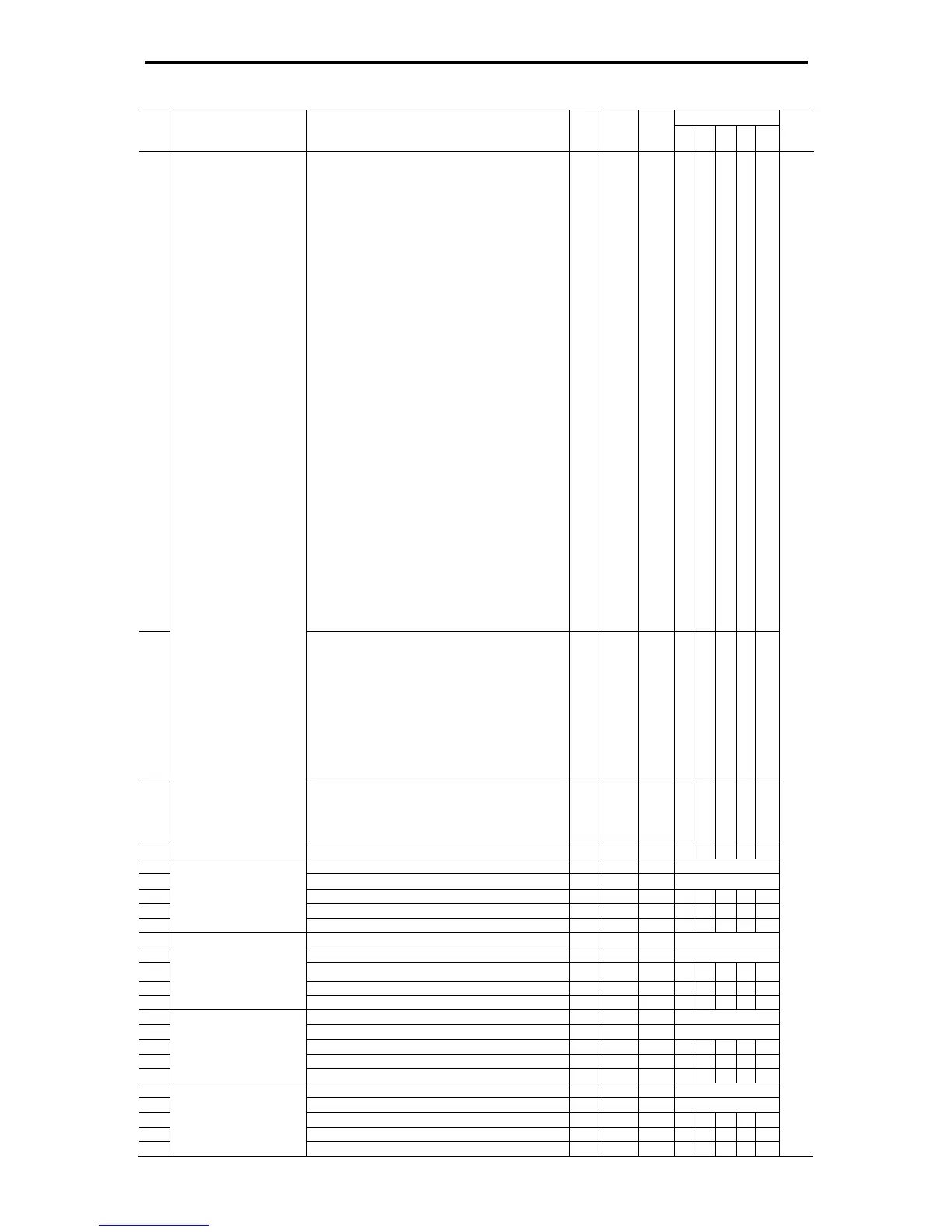
5.2 Function Code Tables
5-24
Drive control
Code Name Data setting range
Change
when
running
Data
copying
Default
setting
V/f
PG
V/f
w/o
PG
w/
PG
To rq ue
control
Refer to
page:
98 (1098): Light alarm (L-ALM) Y Y Y Y Y
99 (1099): Batch alarm processing (ALM) Y Y Y Y Y
105 (1105): Braking transistor broken (DBAL) Y Y Y Y Y
2001 (3001): Output of step 1 (SO01) Y Y Y Y Y
2002 (3002): Output of step 2 (SO02) Y Y Y Y Y
2003 (3003): Output of step 3 (SO03) Y Y Y Y Y
2004 (3004): Output of step 4 (SO04) Y Y Y Y Y
2005 (3005): Output of step 5 (SO05) Y Y Y Y Y
2006 (3006): Output of step 6 (SO06) Y Y Y Y Y 5-249
2007 (3007): Output of step 7 (SO07) Y Y Y Y Y
2008 (3008): Output of step 8 (SO08) Y Y Y Y Y
2009 (3009): Output of step 9 (SO09) Y Y Y Y Y
2010 (3010): Output of step 10 (SO10) Y Y Y Y Y
4001 (5001): Terminal [X1] input signal (X1) Y Y Y Y Y
4002 (5002): Terminal [X2] input signal (X2) Y Y Y Y Y
4003 (5003): Terminal [X3] input signal (X3) Y Y Y Y Y
4004 (5004): Terminal [X4] input signal (X4) Y Y Y Y Y
4005 (5005): Terminal [X5] input signal (X5) Y Y Y Y Y
4006 (5006): Terminal [X6] input signal (X6) Y Y Y Y Y
4007 (5007): Terminal [X7] input signal (X7) Y Y Y Y Y
4008 (5008): Terminal [X8] input signal (X8) Y Y Y Y Y
4009 (5009): Terminal [X9] input signal (X9) Y Y Y Y Y
4010 (5010): Terminal [FWD] input signal (FWD) Y Y Y Y Y
4011 (5011): Terminal [REV] input signal (REV) Y Y Y Y Y
6000 (7000): Final run command (FL_RUN) Y Y Y Y Y
6001 (7001): Final FWD run command (FL_FWD) Y Y Y Y Y
6002 (7002): Final REV run command (FL_REV) Y Y Y Y Y
6003 (7003): During acceleration (DACC) Y Y Y Y Y
6004 (7004): During deceleration (DDEC) Y Y Y Y Y
6005 (7005): Under anti-regenerative control (REGA) Y Y Y Y Y
6006 (7006): Within dancer reference position (DR_REF) Y Y Y Y Y
6007 (7007): Alarm factor presence (ALM_ACT)
* Setting the value in parentheses ( ) shown above assigns a
negative logic output to a terminal. (True if OFF.)
Y Y Y Y Y
U03 (Logic circuit) 0: No function assigned
1: Through output + General-purpose timer
2: ANDing + General-purpose timer
3: ORing + General-purpose timer
4: XORing + General-purpose timer
5: Set priority flip-flop + General-purpose timer
6: Reset priority flip-flop + General-purpose timer
7: Rising edge detector + General-purpose timer
8: Falling edge detector + General-purpose timer
9: Rising & falling edges detector + General-purpose timer
10: Hold + General-purpose timer
11: Increment counter
12: Decrement counter
13: Timer with reset input
N Y 0 Y Y Y Y Y
U04 (Type of timer) 0: No timer
1: On-delay timer
2: Off-delay timer
3: Pulse
4: Retriggerable timer
5: Pulse train output
N Y 0 Y Y Y Y Y
U05 (Time setting) 0.00 to 600.00 N Y 0.00 Y Y Y Y Y
U06 Customizable logic (Input 1) See U01. N Y 0 See U01.
U07 Step 2 (Input 2) See U02. N Y 0 See U02.
U08 (Logic circuit) See U03. N Y 0 Y Y Y Y Y
U09 (Type of timer) See U04. N Y 0 Y Y Y Y Y
U10 (Time setting) See U05. N Y 0.00 Y Y Y Y Y
U11 Customizable logic (Input 1) See U01. N Y 0 See U01.
U12 Step 3 (Input 2) See U02. N Y 0 See U02.
U13 (Logic circuit)
See U03. N Y 0 Y Y Y Y Y
U14 (Type of timer) See U04. N Y 0 Y Y Y Y Y
U15 (Time setting) See U05. N Y 0.00 Y Y Y Y Y
U16 Customizable logic (Input 1) See U01. N Y 0 See U01.
U17 Step 4 (Input 2) See U02. N Y 0 See U02.
U18 (Logic circuit) See U03. N Y 0 Y Y Y Y Y
U19 (Type of timer) See U04. N Y 0 Y Y Y Y Y
U20 (Time setting) See U05. N Y 0.00 Y Y Y Y Y
U21 Customizable logic (Input 1) See U01. N Y 0 See U01.
U22 Step 5 (Input 2) See U02. N Y 0 See U02.
U23 (Logic circuit) See U03. N Y 0 Y Y Y Y Y
U24 (Type of timer) See U04. N Y 0 Y Y Y Y Y
U25 (Time setting) See U05. N Y 0.00 Y Y Y Y Y
 Loading...