52 IBM z13s Technical Guide
2.3.6 Cache level structure
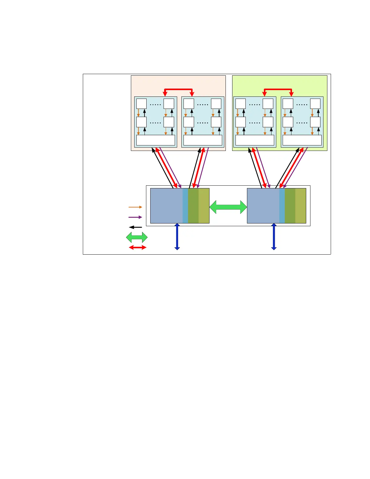
z13s implements a four level cache structure, as shown in Figure 2-16.
Figure 2-16 Cache level structure
Each core has its own 224-KB Level 1 (L1) cache, split into 96 KB for instructions (I-cache)
and 128 KB for data (D-cache). The L1 cache is designed as a store-through cache, meaning
that altered data is also stored in the next level of memory.
The next level is the Level 2 (L2) private cache on each core. This cache has 4 MB, split into
a 2 MB D-cache and 2 MB I-cache. It is designed as a store-through cache.
The Level 3 (L3) cache is also on the PU chip. It is shared by the active cores, has 64 MB, and
is designed as a store-in cache.
Cache levels L2 and L3 are implemented on the PU chip to reduce the latency between the
processor and the L4 large shared cache, which is on the two SC chips. Each SC chip has
480 MB, which is shared by PU chips on the node. The S-bus provide the inter-node interface
between the two L4 caches (SC chips) in each node. The L4 cache uses a store-in design.
Node 0Node 1
64MB eDRAM
Inclusive L3
L1
L2
2MB
L1
L2
2MB
64MB eDRAM
Inclusive L3
L1
L2
2MB
L1
L2
2MB
64MB eDRAM
Inclusive L3
L1
L2
2MB
L1
L2
2MB
64MB eDRAM
Inclusive L3
L1
L2
2MB
L1
L2
2MB
480MB
eDRAM
L4
224MB
eDRAM
NIC
L3
owned
lines
480MB
eDRAM
L4
224MB
eDRAM
NIC
L3
owned
lines
CP Stores
LRU Cast-out
Data Fetch Return
S-Bus
X-Bus
To other CPC drawer
PU chip (7 cores) PU chip (6 cores) PU chip (6 cores) PU chip (7 cores)