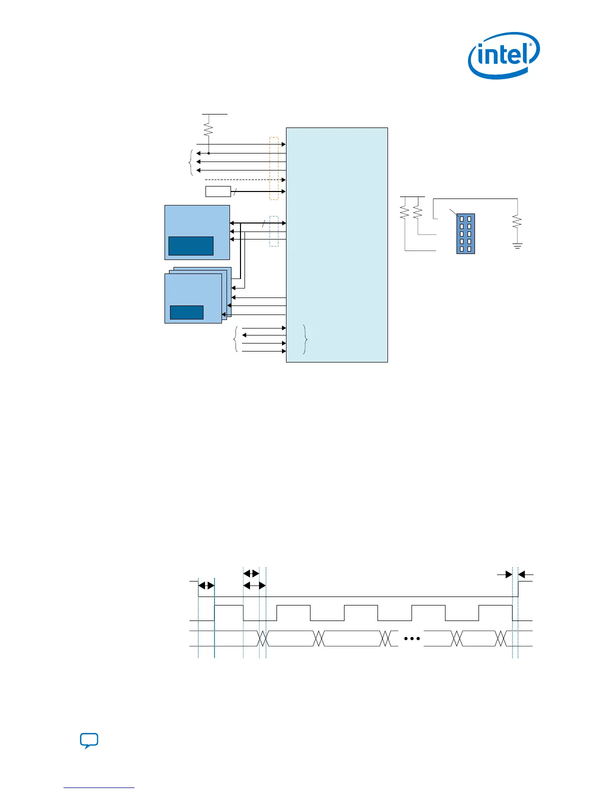
Figure 22. Connection Setup for AS Configuration with Multiple Serial Flash Devices
Pin 1
R
UP
R
DN
R
UP
TCK
TDO
TMS
OPEN
TDI
GND
VCCIO_SDM
OPEN
OPEN
GND
G
ND
V
CCIO_SDM
Intel® Stratix®10
nCONFIG
nSTATUS
CONF_DONE
INIT_DONE
OSC_CLK_1
MSEL[2:0]
AS_DATA[3:0]
Config AS x4 Memory
AS_CLK
AS_nCS0[0]
AS_nCS0[1]
AS_nCS0[2]
AS_nCS0[3]
Download cable 10 pin male header (JTAG mode)
DATA[3:0]
DCLK
CS
Configuration
Control Signals
Configuration
Data Signals
Optional
Monitoring
10kΩ
Optional
HPS Data Signals
MSEL
V
CCIO_SDM
3
4
To JTAG Header
or JTAG Chain
TCK
TDO
TDI
TMS
JTAG
Configuration
Pins
FPGA
Image (.jic)
HPS AS x4 Memory
DATA[3:0]
DCLK
CS
HPS Data
3M Part number : 2510-6002UB
To allow the JTAG interface to program the flash memory devices, set the MSEL pins to
JTAG. When MSEL is set to JTAG, the SDM tristates the AS pins, AS_CLK, AS_DATA0-
AS_DATA3, and AS_CS0-AS_CS3, when the device powers on.
Note: When using multiple flash devices, the clock frequency must be reduced. Refer to the
Intel Stratix 10 Device Datasheet for more information.
Related Information
• MSEL Settings on page 18
• Intel Stratix 10 Device Datasheet (Core and HPS)
• Intel Stratix 10 Device Family Pin Connection Guidelines
3.2.3. AS Configuration Timing
Figure 23. AS Configuration Serial Output Timing Diagram
nCSO
AS_CLK
AS_DATA
OUT0 OUT1
OUTn
T
dcslst
T
dcsfrs
T
do (max)
T
do (min)
3. Intel Stratix 10 Configuration Schemes
UG-S10CONFIG | 2018.11.02
Send Feedback
Intel Stratix 10 Configuration User Guide
53
 Loading...