12. Timer B
puorG92/C61M
page 124
854fo7002,03.raM21.1.veR
2110-1010B90JER
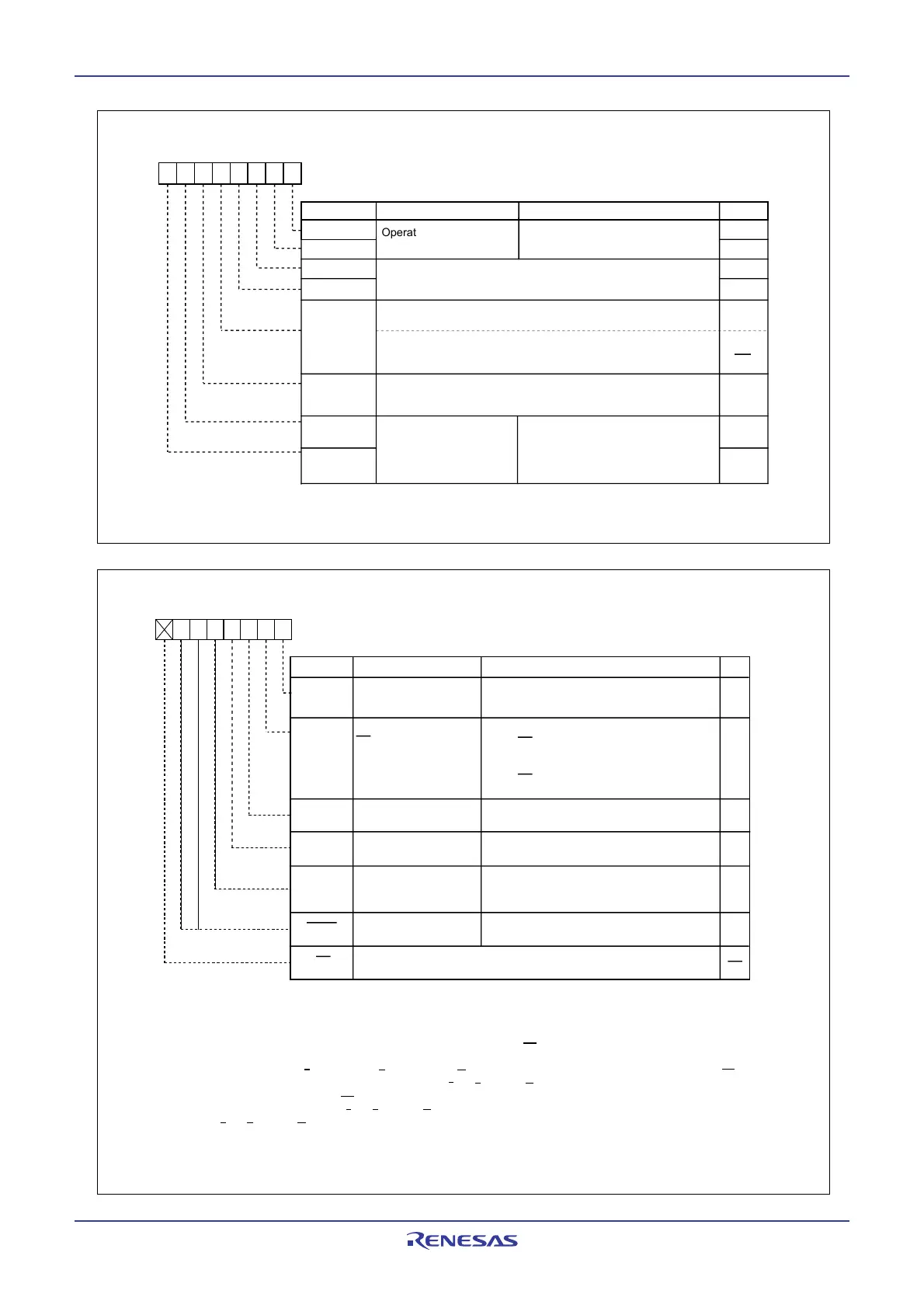
Figure 12.23 TBiMR Register in A/D Trigger Mode
Figure 12.24 TB2SC Register in A/D Trigger Mode
Timer Bi Mode Register (i= 0 to 1)
Symbol Address After Reset
TB0MR to TB1MR 039B
16
to 039C
16
00XX0000
2
Bit Name
Function
Bit Symbol
RW
b7 b6 b5 b4 b3 b2 b1 b0
Operation mode select bit
0 0: Timer mode or A/D trigger mode
b1 b0
TMOD1
TMOD0
MR0
Invalid in A/D trigger mode
Either 0 or 1 is enabled
MR2
MR1
MR3
0 0: f
1
or f
2
0 1: f
8
1 0: f
32
1 1: f
C32
TCK1
TCK0
Count source select bit
00
TB0MR register
Set to 0 in A/D trigger mode
b7 b6
RO
TB1MR register
Nothing is assigned. If necessary, set to 0. When read, its
content is undefined
When write in A/D trigger mode, set to 0. When read in A/D trigger
mode, its content is undefined
NOTE:
1. When this bit is used in delayed trigger mode 0, set the same count source to the timer B0 and timer B1.
(1)
RW
RW
RW
RW
RW
RW
RW
PWCON
Symbol Address
TB2SC 039E
16
X0000000
2
Timer B2 reload timing
switch bit
0: Timer B2 underflow
1: Timer A output at odd-numbered
Timer B2 special mode register
(1)
Bit Name FunctionBit Symbol
b7 b6 b5 b4 b3 b2 b1 b0
IVPCR1
Three-phase output port
SD control bit 1
0: Three-phase output forcible cutoff
by SD pin input (high impedance)
disabled
1: Three-phase output forcible cutoff
by SD pin input (high impedance)
enabled
RW
RW
RW
Nothing is assigned. If necessary, set to 0.
When read, its content is 0
(b7)
TB2SEL
Trigger select bit
0: TB2 interrupt
1: Underflow of TB2 interrupt
generation frequency setting counter [ICTB2]
RW
RW
TB0EN
Timer B0 operation mode
select bit
0: Other than A/D trigger mode
1: A/D trigger mode
RW
TB1EN
Timer B1 operation mode
select bit
0: Other than A/D trigger mode
1: A/D trigger mode
RW
(2)
(3, 4, 7)
(5)
(5)
(6)
(b6-b5)
Reserved bits
Set to 0
00 11
After Reset
NOTES:
1. Write to this register after setting the PRC1 bit in the PRCR register to 1 (write enabled).
2. If the INV11 bit is 0 (three-phase mode 0) or the INV06 bit is 1 (triangular wave modulation mode), set this bit to 0 (timer
B2 underflow).
3. When setting the IVPCR1 bit to 1 (three-phase output forcible cutoff by SD pin input enabled), Set the PD8
5
bit to 0 (= input
mode).
4. Related pins are U(P8
0), U(P81), V(P72), V(P73), W(P74), W(P75). When a high-level ("H") signal is applied to the SD pin
and set the IVPCR1 bit to 0 after forcible cutoff, pins U, U, V, V, W, and W are exit from the high-impedance state. If a low-
level (“L”) signal is applied to the SD pin, three-phase motor control timer output will be disabled (INV03=0). At this time,
when the IVPCR1 bit is 0, pins U, U, V, V, W, and W become programmable I/O ports. When the IVPCR1 bit is set to 1,
pins U, U, V, V, W, and W are placed in a high-impedance state regardless of which function of those pins is used.
5. When this bit is used in delayed trigger mode 0, set bits TB0EN and TB1EN to 1 (A/D trigger mode).
6. When setting the TB2SEL bit to 1 (underflow of TB2 interrupt generation frequency setting counter[ICTB2]), set the INV02
bit to 1 (three-phase motor control timer function).
 Loading...


