15. A/D Converter
puorG92/C61M
page 254
854fo7002,03.raM21.1.veR
2110-1010B90JER
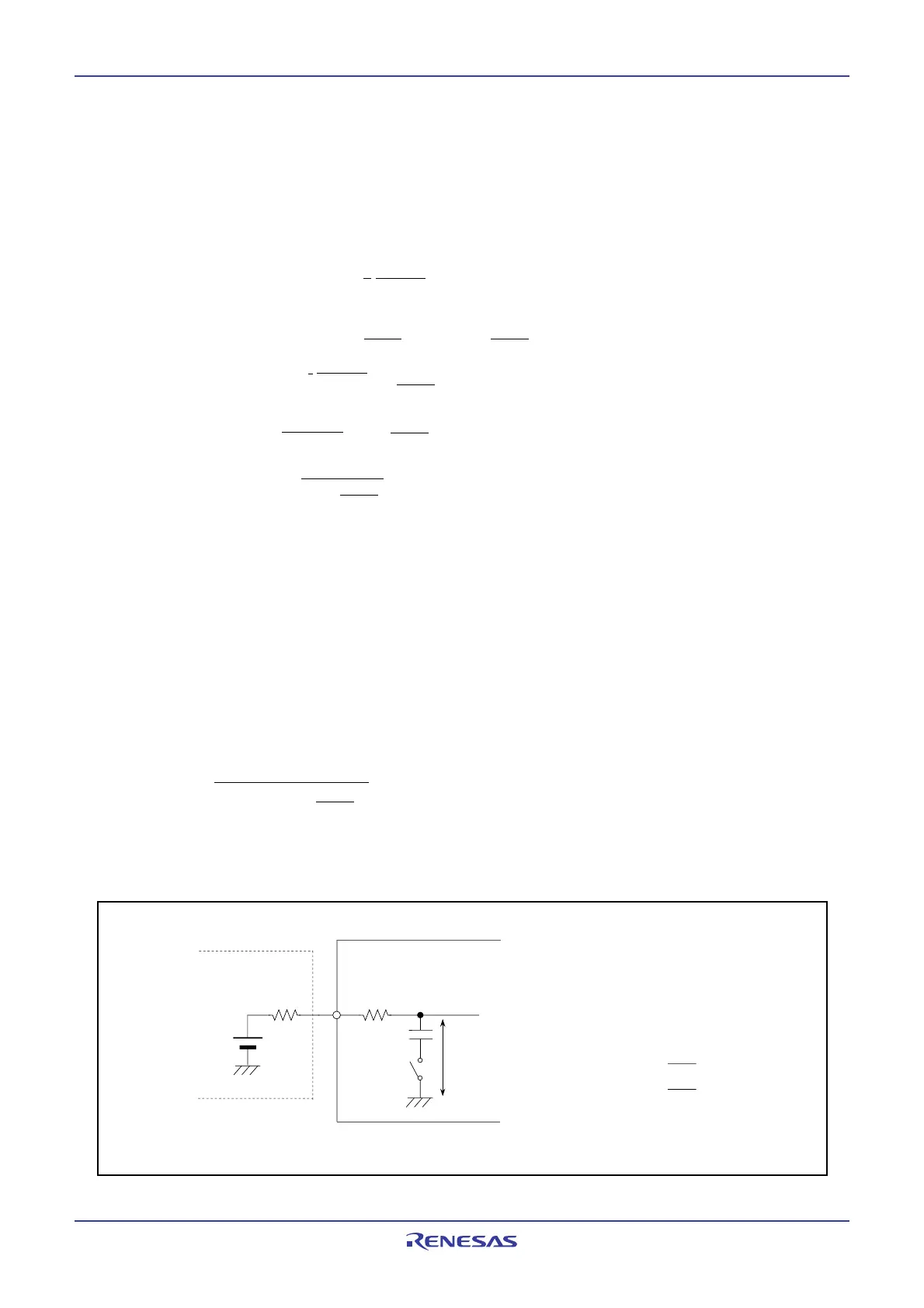
Figure 15.29 Analog Input Pin and External Sensor Equivalent Circuit
15.5 Output Impedance of Sensor under A/D Conversion
To carry out A/D conversion properly, charging the internal capacitor C shown in Figure 15.29 has to be
completed within a specified period of time. T (sampling time) as the specified time. Let output imped-
ance of sensor equivalent circuit be R0, MCU’s internal resistance be R, precision (error) of the A/D
converter be X, and the A/D converter’s resolution be Y (Y is 1024 in the 10-bit mode, and 256 in the 8-
bit mode).
VC is generally VC = VIN{1-e
c(R0+R)
}
And when t = T, VC=VIN- VIN=VIN(1- )
e
c(R0+R)
=
- T = ln
Hence, R0 = - - R
Figure 15.29 shows analog input pin and externalsensor equivalent circuit. When the difference be-
tween VIN and VC becomes 0.1 LSB, we find impedance R0 when voltage between pins. VC changes
from 0 to VIN-(0.1/1024) VIN in timer T. (0.1/1024) means that A/D precision drop due to insufficient
capacitor chage is held to 0.1LSB at time of A/D conversion in the 10-bit mode. Actual error however is
the value of absolute precision added to 0.1LSB. When f(XIN) = 10MHz, T=0.3µs in the A/D conversion
mode with sample & hold. Output inpedance R0 for sufficiently charging capacitor C within time T is
determined as follows.
T = 0.3µs, R = 7.8kΩ, C = 1.5pF, X = 0.1, and Y = 1024. Hence,
R0 = - - 7.8 X 10
3
≅ 13.9 X 10
3
Thus, the allowable output impedance of the sensor circuit capable of thoroughly driving the A/D con-
verter turns out of be approximately 13.9kΩ.
1
1
T
t
C(R0+R)
1
X
Y
X
Y
X
Y
X
Y
T
C•ln
X
Y
1.5X10
-12
•ln
0.1
1024
0.3X10
-6
R0
R (7.8kΩ)
C (1.5pF)
VIN
VC
Sampling time
Sample-and-hold function enabled:
Sample-and-hold function disabled:
3
φ
AD
MCU
Sensor equivalent
circuit
2
φ
AD
(1)
(1)
NOTE:
1. Reference value
 Loading...


