16. MULTI-MASTER I
2
C bus INTERFACE
puorG92/C61M
page 264
854fo7002,03.raM21.1.veR
2110-1010B90JER
16.2 I
2
C0 Address Register (S0D0 register)
The S0D0 register consists of bits SAD6 to SAD0, total of 7. At the addressing is formatted, slave
address is detected automatically and the 7-bit received address data is compared with the contents of
bits SAD6 to SAD0.
16.1 I
2
C0 Data Shift Register (S00 register)
The S00 register is an 8-bit data shift register to store a received data and to write a transmit data. When a
transmit data is written to the S00 register, the transmit data is synchronized with a SCL clock and the data
is transferred from bit 7. Then, every one bit of the data is transmitted, the register's content is shifted for
one bit to the left. When the SCL clock and the data is imported into the S00 register from bit 0. Every one
bit of the data is imported, the register's content is shifted for one bit to the left. Figure 16.9 shows the
timing to store the receive data to the S00 register.
The S00 register can be written when the ES0 bit in the S1D0 register is set to 1 (I
2
C0 bus interface
enabled). If the S00 register is written when the ES0 bit is set to 1 and the MST bit in the S10 register is set
to 1 (master mode), the bit counter is reset and the SCL clock is output. Write to the S00 register when the
START condition is generatedor when an "L" signal is applied to the SCL pin. The S00 register can be read
anytime regardless of the ES0 bit value.
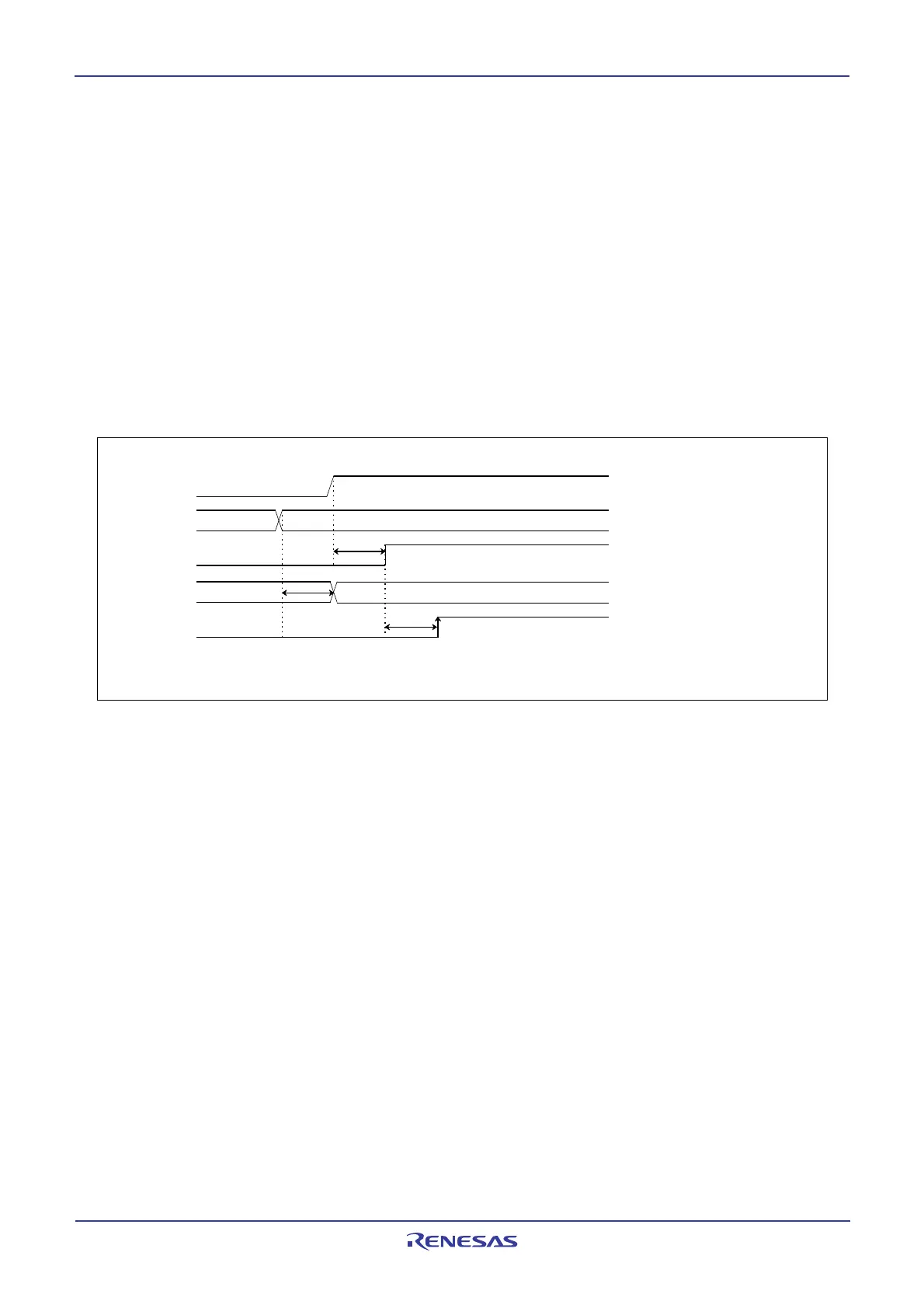
Figure 16.9 The Receive Data Storing Timing of S00 Register
Internal S
CL
tdfil
Store data at the rising edge of shift clock
Internal S
DA
Shift clock
S
CL
S
DA
tdfil
tdsft
tdfil: Noise elimination circuit delay time
1 to 2 V
IIC
cycle
tdsft: Shift clock delay time
1 V
IIC
cycle
 Loading...


