6. Processor Mode
puorG92/C61M
page 44
854fo7002,03.raM21.1.veR
2110-1010B90JER
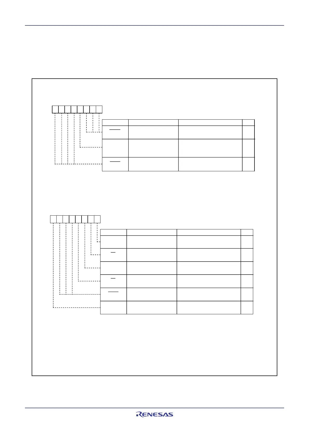
Processor Mode Register 1
(1)
Symbol Address After Reset
PM1 0005
16
00001000
2
Bit Name FunctionBit Symbol
RW
b7 b6 b5 b4 b3 b2 b1 b0
Flash data block access
bit
(2)
0: Disabled
1: Enabled
(3)
PM10
RW
PM17 Wait bit
(5)
0 : No wait state
1 : Wait state (1 wait)
0 : Watchdog timer interrupt
1 : Watchdog timer reset
(4)
Watchdog timer function
select bit
PM12
RW
RW
RW
RW
RW
NOTES:
1. Rewrite the PM1 register after the PRC1 bit in the PRCR register is set to 1 (write enable).
2. To access the two 2K-byte data spaces in data block A and data block B, set the PM10 bit to 1. The PM10
bit is not available in mask version.
3. When the FMR01 bit in the FMR0 register is set to 1 (enables CPU rewrite mode), the PM10 bit is
automatically set to 1.
4. Set the PM12 bit to 1 by program. (Writing 0 by program has no effect)
5. When the PM17 bit is set to 1 (wait state), one wait is inserted when accessing the internal RAM or the
internal ROM.
Set to 0
(b1)
Reserved bit
Set to 1Reserved bit
Set to 0
(b6-b4)
Reserved bit
(b3)
0
1
0
00
6. Processor Mode
The MCU supports single-chip mode only. Figures 6.1 and 6.2 show the associated registers.
Figure 6.1 PM0 Register and PM1 Register
Processor Mode Register 0
(1)
Symbol Address After Reset
PM0 0004
16
00
16
Bit Name FunctionBit Symbol
RW
b7 b6 b5 b4 b3 b2 b1 b0
The MCU is reset when
this bit is set to 1. When read,
its content is 0.
Software reset bitPM03
RW
RW
RW
NOTES:
1. Set the PM0 register after the PRC1 bit in the PRCR register is set to 1 (write enable).
Set to 0
(b2-b0)
Reserved bit
Set to 0
(b7-b4)
Reserved bit
0000000
 Loading...


