5. Resets
puorG92/C61M
page 41
854fo7002,03.raM21.1.veR
2110-1010B90JER
5.5.1 Low Voltage Detection Interrupt
If the D40 bit in the D4INT register is set to 1 (low voltge detection interrupt enabled), a low voltage
detection interrupt request is generated when voltage applied to the VCC pin is above or below Vdet4.
The low voltage detection interrupt shares the same interrupt vector with watchdog timer interrupt and
oscillation stop, re-oscillation detection interrupt.
Set the D41 bit in the D4INT register to 1 (enabled) to use the low voltage detection interrupt to exit stop
mode, set the D41 bit in the D4INT register to 1 (enable).
The D42 bit in the D4INT register is set to 1 (above or below Vdet4 detected) as soon as voltage applied
to the VCC pin goes above or below Vdet4 due to the voltage change. When the D42 bit setting changes
0 to 1, a low voltage detection interrupt is generated. Set the D42 bit to 0 (not detected) by program.
However, when the D41 bit is set to 1 and the MCU is in stop mode, a low voltage detection interrupt
request is generated, regardless of the D42 bit setting, if voltage applies to the VCC pin is detected to rise
above or drop below Vdet4. The MCU then exits stop mode.
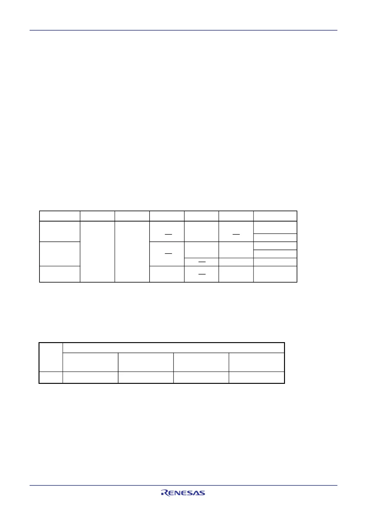
Table 5.2 shows how a low voltage detection interrupt request is generated.
Bits DF1 and DF0 in the D4INT register determine sampling period that detects voltage applied to the
VCC pin rises above or drops below Vdet4. Table 5.3 shows sampling periods.
Table 5.2 Voltage Detection Interrupt Request Generation Conditions
Table 5.3 Sampling Clock Periods
D41 bitVC27 bitOperation Mode D40 bit D42 bit CM02 bit VC13 bit
Normal
operation
mode(1)
Wait mode
(2)
Stop mode
(2)
NOTES:
1. The status except the wait mode and stop mode is handled as the normal mode. (Refer to 7. Clock generating circuit)
2. Refer to 5.5.2 Limitations on stop mode and 5.5.3 Limitations on wait mode.
3. An interrupt request for voltage reduction is generated a sampling time after the value of the VC13 bit has changed.
Refer to the Figure 5.9 for details.
0 to 1
1
0
1
1
0
1 to 0
0 to 1
1 to 0
0 to 1
0 to 1
0 to 1
0 to 1
1
(3)
– : 0 or 1
(3)
(3)
(3)
CPU
clock
(MHz)
DF1 to DF0=00
(CPU clock divided by 8)
Sampling clock (µs)
16 3.0 6.0 12.0 24.0
DF1 to DF0=01
(CPU clock divided by 16)
DF1 to DF0=10
(CPU clock divided by 32)
DF1 to DF0=11
(CPU clock divided by 64)
 Loading...


