16. MULTI-MASTER I
2
C bus INTERFACE
puorG92/C61M
page 274
854fo7002,03.raM21.1.veR
2110-1010B90JER
16.6.6 Address Receive in STOP/WAIT Mode
When WAIT mode is entered after the CM02 bit in the CM0 register is set to 0 (do not stop the peripheral
function clock in wait mode), the I
2
C bus interface circuit can receive address data in WAIT mode. How-
ever, the I
2
C bus interface circuit is not operated in STOP mode or in low power consumption mode,
because the I
2
C bus system clock VIIC is not supplied.
16.6.4 Bits 4,5 : SDA/SCL Logic Output Value Monitor Bits SDAM/SCLM
Bits SDAM/SCLM can monitor the logic value of the SDA and SCL output signals from the I
2
C bus
interface circuit. The SDAM bit monitors the SDA output logic value. The SCLM bit monitors the SCL
output logic value. The SDAM and SCLM bits are read-only. If necessary, set them to 0.
16.6.5 Bits 6,7 : I
2
C System Clock Select Bits ICK0, ICK1
The ICK1 bit, ICK0 bit, bits ICK4 to ICK2 in the S4D0 register, and the PCLK0 bit in the PCLKR register
can select the system clock (VIIC) of the I
2
C bus interface circuit.
The I
2
C bus system clock VIIC can be selected among 1/2 fIIC, 1/2.5 fIIC, 1/3 fIIC, 1/4 fIIC, 1/5 fIIC, 1/6 fIIC
and 1/8 fIIC. fIIC can be selected between f1 and f2 by the PCLK0 bit setting.
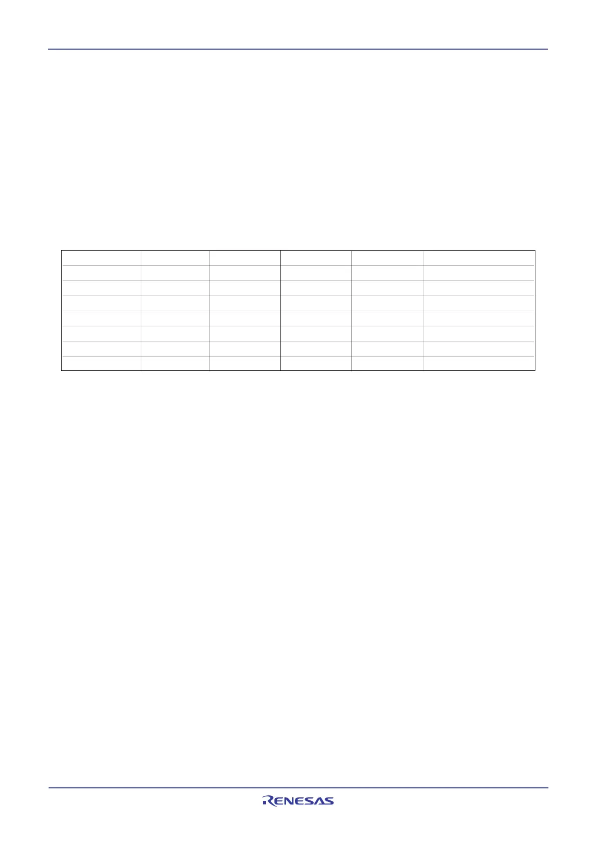
I3CK4[S4D0] ICK3[S4D0] ICK2[S4D0] ICK1[S3D0] ICK0[S3D0] I
2
C system clock
00000VIIC = 1/2 fIIC
00001VIIC = 1/4 fIIC
00010VIIC = 1/8 fIIC
001XXVIIC = 1/2.5 fIIC
010XXVIIC = 1/3 fIIC
011XXVIIC = 1/5 fIIC
100XXVIIC = 1/6 fIIC
Table 16.6 I
2
C system clock select bits
( Do not set the combination other than the above)
 Loading...


