15. A/D Converter
puorG92/C61M
page 234
854fo7002,03.raM21.1.veR
2110-1010B90JER
Item Specification
Function Bits SCAN1 and SCAN0 in the ADCON1 register and bits ADGSEL1 and
ADGSEL0 in the ADCON2 register select pins. Analog voltage applied to the
selected pins is repeatedly converted to a digital code
A/D Conversion Start Condition
• When the TRG bit in the ADCON0 register is 0 (software trigger)
Set the ADST bit in the ADCON0 register to 1 (A/D conversion started)
• When the TRG bit in the ADCON0 register is 1 (Hardware trigger)
The ADTRG pin input changes state from “H” to “L” after setting the ADST bit
to 1 (A/D conversion started)
A/D Conversion Stop Condition
Set the ADST bit to 0 (A/D conversion halted)
Interrupt Request Generation Timing
None generated
Analog Input Pin Select from AN0 to AN1 (2 pins), AN0 to AN3 (4 pins), AN0 to AN5 (6 pins),
AN0 to AN7 (8 pins)
(1)
Readout of A/D Conversion Result
Readout one of registers AD0 to AD7 that corresponds to the selected pin
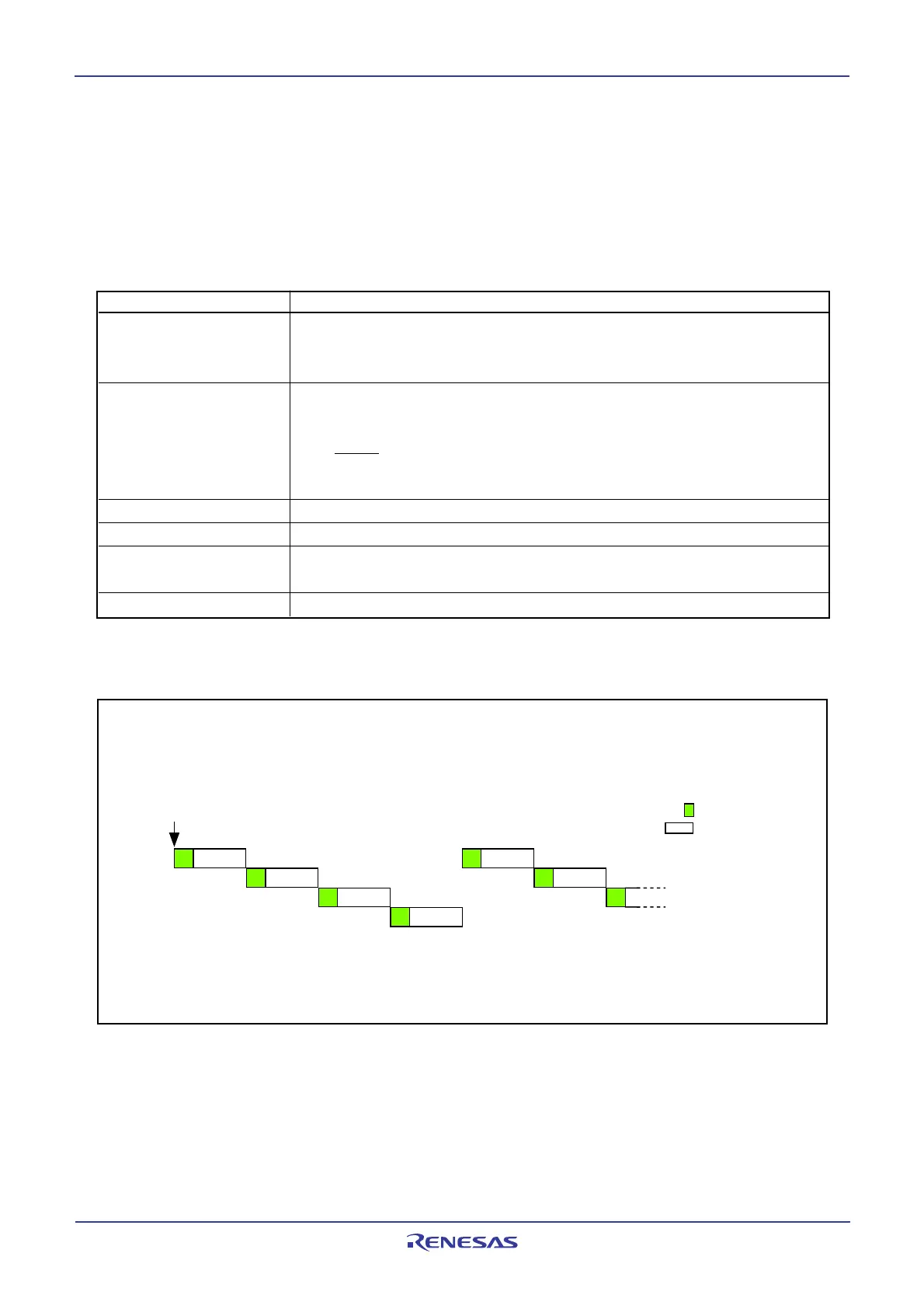
15.1.4 Repeat Sweep Mode 0
In repeat sweep mode 0, analog voltages applied to the selected pins are repeatedly converted to a
digital code. Table 15.6 shows the repeat sweep mode 0 specifications. Figure 15.12 shows the opera-
tion example in repeat sweep mode 0. Figure 15.13 shows the ADCON0 to ADCON2 registers in repeat
sweep mode 0.
Table 15.6 Repeat Sweep Mode 0 Specifications
NOTES:
1. AN00 to AN07, AN 20 to AN27, and
AN3
0
to AN3
2
can be used in the same way as AN0 to AN7.
However, all input pins need to belong to the same group.
Figure 15.12 Operation Example in Repeat Sweep Mode 0
•Example when selecting AN0 to AN3 to A/D sweep pins (SCAN1 to SCAN0 = 012)
A/D conversion started
AN0
AN1
AN2
AN3
AN4
AN5
AN6
AN7
A/D pin input voltage
sampling
A/D pin conversion
 Loading...


