5. Resets
puorG92/C61M
page 40
854fo7002,03.raM21.1.veR
2110-1010B90JER
Figure 5.7 Typical Operation of Brown-Out Detection Reset (Hardware Reset 2)
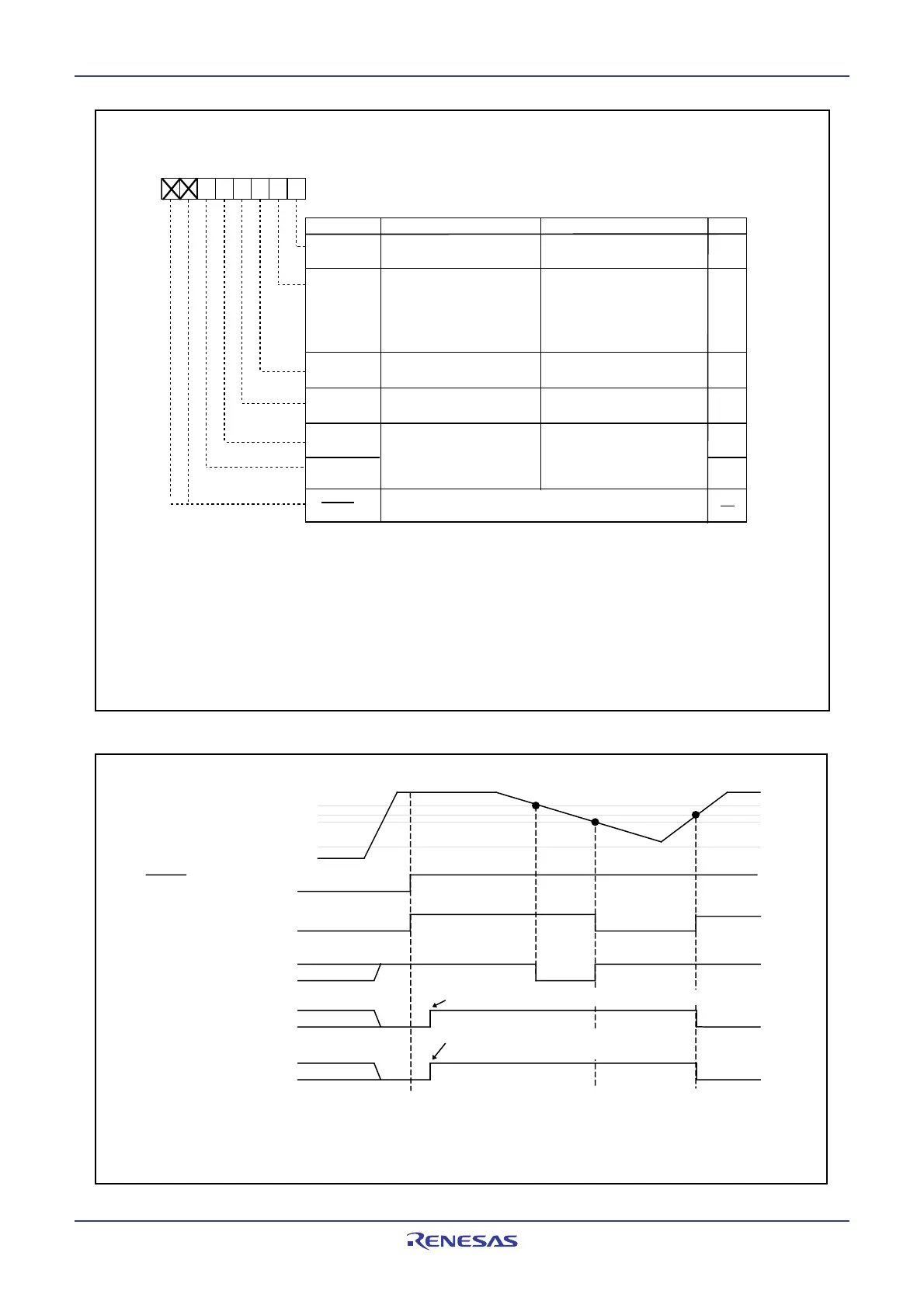
Figure 5.6 D4INT Register
D
4
0
Lo
w
V
o
l
t
a
g
e
D
e
t
e
c
t
i
o
n
I
n
t
e
r
r
u
p
t
R
e
g
i
s
t
e
r
(
1
)
Symbol Address After Reset
D4INT 001F
16
00
16
Low voltage detection
interrupt enable bit
(5)
B
i
t
N
a
m
e
Bit Symbol
b7 b
6
b
5
b
4
b
3
b
2
b
1
b
0
0
:
D
i
s
a
b
l
e
1
:
E
n
a
b
l
e
D
4
1
S
T
O
P
m
o
d
e
d
e
a
c
t
i
v
a
t
i
o
n
c
o
n
t
r
o
l
b
i
t
(
4
)
0: Disable (do not use the low
voltage detection interrupt to exit
stop mode)
1: Enable (use the low voltage
detection interrupt to exit stop
mode)
D
4
2
V
o
l
t
a
g
e
c
h
a
n
g
e
d
e
t
e
c
t
i
o
n
f
l
a
g
(
2
)
0
:
N
o
t
d
e
t
e
c
t
e
d
1
:
V
d
e
t
4
p
a
s
s
i
n
g
d
e
t
e
c
t
i
o
n
D
4
3
W
D
T
o
v
e
r
f
l
o
w
d
e
t
e
c
t
f
l
a
g
0: Not detected
1: Detected
D
F
0
S
a
m
p
l
i
n
g
c
l
o
c
k
s
e
l
e
c
t
b
i
t
00 : CPU clock divided by 8
01 : CPU clock divided by 16
10 : CPU clock divided by 32
11 : CPU clock divided by 64
DF1
NOTES:
1. Write to this register after setting the PRC3 bit in the PRCR register to 1 (write enable).
2. Useful when the VC27 bit in the VCR2 register is set to 1 (low voltage detection circuit enabled). If the VC27
bit is set to 0 (low voltage detection circuit disable), the D42 bit is set to 0 (Not detect).
3. This bit is set to 0 by writing a 0 in a program. (Writing 1 has no effect.)
4. If the low voltage detection interrupt needs to be used to get out of stop mode again after once used for that
purpose, reset the D41 bit by writing a 0 and then a 1.
5. The D40 bit is effective when the VC27 bit in the VCR2 register is set to 1. To set the D40 bit to 1, follow the
procedure described below.
(1) Set the VC27 bit to 1.
(2) Wait for td(E-A) until the detection circuit is actuated.
(3) Wait for the sampling time (refer to Table 5.3 Sampling Clock Periods).
(4) Set the D40 bit to 1.
5
4
R
W
R
W
R
W
R
W
3
R
W
R
W
RW
(
b
7
-
b
6
)
Function
3
N
o
t
h
i
n
g
i
s
a
s
s
i
g
n
e
d
.
I
f
n
e
c
e
s
s
a
r
y
s
e
t
t
o
0
.
W
h
e
n
r
e
a
d
,
t
h
e
c
o
n
t
e
n
t
i
s
0
Vdet4
Vdet3
5.0V
5.0V
VCC
Internal Reset Signal
VC13 bit in
VCR1 register
VC26 bit in
VCR2 register
(1)
VC27 bit in
VCR2 register
Set to 1 by program (reset level detect circuit enable)
Set to 1 by program
(low voltage detection circuit enable)
VSS
Undefined
RESET
Vdet3s
Vdet3r
NOTES :
1. VC26 bit is invalid in stop mode. (the MCU is not reset even if input voltage of VCC pin
becomes lower than Vdet3).
Undefined
Undefined
 Loading...


