14. Serial I/O
puorG92/C61M
page 218
854fo7002,03.raM21.1.veR
2110-1010B90JER
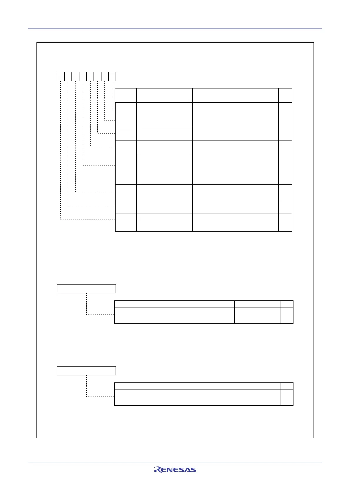
Figure 14.36
S3C and S4C Registers, S3BRG and S4BRG Registers, and S3TRR and S4TRR Registers
7
0
Symbol Address After Reset
S3BRG 0363
16 Undefined
S4BRG 0367
16 Undefined
0
0
1
6
t
o
F
F1
6
7
0
Symbol Address After Reset
S3TRR 0360
16 Undefined
S4TRR 0364
16 Undefined
S
y
m
b
o
lA
d
d
r
e
s
sA
f
t
e
r
R
e
s
e
t
S
3
C0
3
6
2
1
6 0
1
0
0
0
0
0
02
S
4
C0
3
6
61
6 0
1
0
0
0
0
0
02
b
7b
6b
5b
4b
3b
2b
1b
0
RW
Function
SMi5
S
M
i
1
SMi0
S
M
i
3
SMi6
S
M
i
7
Internal synchronous clock
select bit
Transfer direction select bit
S
I
/
O
i
p
o
r
t
s
e
l
e
c
t
b
i
t
S
O
U
Ti
i
n
i
t
i
a
l
v
a
l
u
e
s
e
t
b
i
t
0 0 : Selecting f
1 or f2
0 1 : Selecting f8
1 0 : Selecting f32
1 1 : Do not set
b1 b0
0 : External clock
(2)
1 : Internal clock
(3)
Effective when the SMi3 is set to 0
0 : “L” output
1 : “H” output
0 : Input/output port
1 : S
OUTi output, CLKi function
Bit Name
B
i
t
S
y
m
b
o
l
Synchronous clock select bit
0 : LSB first
1 : MSB firs
t
S
M
i
2S
O
U
Ti
o
u
t
p
u
t
d
i
s
a
b
l
e
b
i
t0 : SOUTi output
1 : S
OUTi output disable(high impedance)
S
M
i
4C
L
K
p
o
l
a
r
i
t
y
s
e
l
c
t
b
i
t
0 : Transmit data is output at falling edge of
transfer clock and receive data is input at
rising edge
1 : Transmit data is output at rising edge of
transfer clock and receive data is input at
falling edg
e
RW
RW
RW
RW
RW
RW
RW
RW
RW
RW
RW
W
O
4
5
NOTES:
1. Set the S4C register by the next instruction after setting the PRC2 bit in the PRCR register to 1 (write enable).
2. Set the SMi3 bit to 1 and the corresponding port direction bit to 0 (input mode).
3. Set the SMi3 bit to 1 (SOUTi output, CLKi function) .
4. When the SMi2 bit is set to 1, the corresponding pin goes to high-impedance regardless of the function in use.
5. When the SMi1 and SMi0 bit settings are changed, set the SiBRG register .
NOTES:
1. Write to this register while serial I/O is neither transmitting or receiving.
2. To receive data, set the corresponding port direction bit for S
INi to 0 (input mode).
NOTES:
1. Write to this register while serial I/O is neither transmitting or receiving.
2. Use MOV instruction to write to this register.
3. Set the SiBRG register after setting bits SMi1 and SMi0 in the SiC register.
Transmission/reception starts by writing transmit data to this register. After
transmission/reception completion, reception data can be read by reading this register.
Assuming that set value = n, BRGi divides the count source by
n + 1
Setting RangeDescription
Description
SI/Oi Control Register (i = 3, 4)
(1)
SI/Oi Bit Rate Generation Register (i = 3, 4)
(1, 2, 3)
SI/Oi Transmit/Receive Register (i = 3, 4)
(1, 2)
 Loading...


