1. Overview
page 2
puorG92/C61M
854fo7002,03.raM21.1.veR
2110-1010B90JER
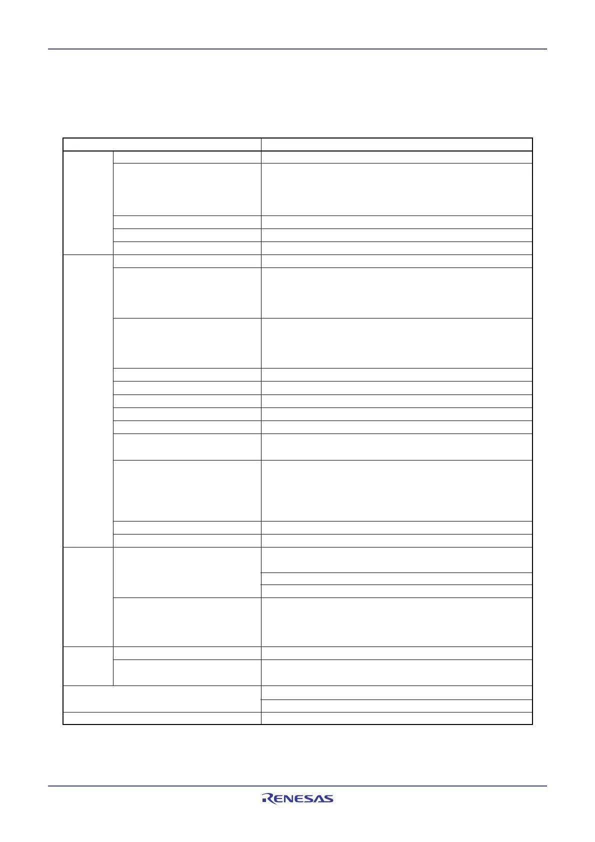
Item Performance
CPU Number of basic instructions 91 instructions
Shortest instruction
50 ns (f(BCLK) = 20MHZ, VCC = 3.0 to 5.5 V) (Normal-ver./T-ver.)
excution time
100 ns(f(BCLK) = 10MHZ, VCC = 2.7 to 5.5 V) (Normal-ver.)
50 ns (f(BCLK) = 20MHZ, VCC = 4.2 to 5.5 V, -40 to 105°C) (V-ver.)
62.5 ns (f(BCLK) = 16MHZ, VCC = 4.2 to 5.5 V, -40 to 125°C) (V-ver.)
Operation mode Single chip mode
Address space 1 Mbyte
Memory capacity ROM/RAM: See Tables 1.3 to 1.5
Peripheral
Port Input/Output: 71 lines
Function Multifunction timer TimerA:16 bits x 5 channels, TimerB:16 bits x 3 channels
Three-phase Motor Control Timer
TimerS (Input Capture/Output Compare):
16 bit base timer x 1 channel (Input/Output x 8 channels
)
Serial I/O 2 channels (UART, clock synchronous serial I/O)
1 channel (
UART, clock synchronous serial I/O, I
2
C bus, or IEbus
(1)
)
2 channels (Clock synchronous serial I/O)
1 channel (Multi- master I
2
C bus)
A/D converter 10 bits x 27 channels
DMAC 2 channels
CRC calculation circuit
2 polynomial (CRC-CCITT and CRC-16) with MSB/LSB selectable
CAN module 1 channel, supporting CAN 2.0B specification
Watchdog timer 15 bits x 1 channel (with prescaler)
Interrupt 29 internal and 8 external sources, 4 software sources,
interrupt priority level: 7
Clock generation circuit 4 circuits
• Main clock
• Sub-clock
•
On-chip oscillator
(main-clock oscillation stop detect function)
• PLL frequency synthesizer
Oscillation stop detect Function Main clock oscillation stop, re-oscillation detect function
Voltage detection circuit Available (Normal-ver.) / Not available (T-ver., V-ver.)
Electrical
Power supply voltage VCC = 3.0 to 5.5 V (f(BCLK) = 20 MHz) (Normal-ver.)
Charact-
VCC = 2.7 to 5.5 V (f(BCLK) = 10 MHz)
eristics
VCC = 3.0 to 5.5 V (T-ver.)
VCC = 4.2 to 5.5 V (V-ver.)
Power consumption 18 mA (VCC = 5 V, f(BCLK) = 20 MHz)
25 µA (f(XCIN) = 32 kHz on RAM)
3 µA (VCC = 5 V, f(XCIN) = 32 kHz, in wait mode)
0.8 µA (VCC = 5 V, in stop mode)
Flash
Program/erase supply voltage
2.7 to 5.5 V (Normal-ver.), 3.0 to 5.5V (T-ver.), 4.2 to 5.5 V (V-ver.)
memory
Program and erase endurance
100 times (all space) or 1,000 times (blocks 0 to 5)/
10,000 times (blocks A and B
(2)
)
Operating ambient temperature -20 to 85°C/-40 to 85°C
(2)
(Normal-ver.)
-40 to 85°C (T-ver.), -40 to 125°C (V-ver.)
Package 80-pin plastic mold LQFP
Table 1.1 Performance Overview of M16C/29 Group (T-ver./V-ver.) (80-Pin Package)
1.1.2 Specifications
Table 1.1 lists performance overview of M16C/29 Group 80-pin package.
Table 1.2 lists performance overview of M16C/29 Group 64-pin package.
(These circuits contain a built-in feedback
resistor)
NOTES:
1. IEBus is a trademark of NEC Electronics Corporation.
2. Refer to Table 1.6 to Table 1.8 Product code.
 Loading...


