Clock-Asynchronous Serial I/O
M30240 Group
Rev.1.00 Sep 24, 2003 Page 223 of 360
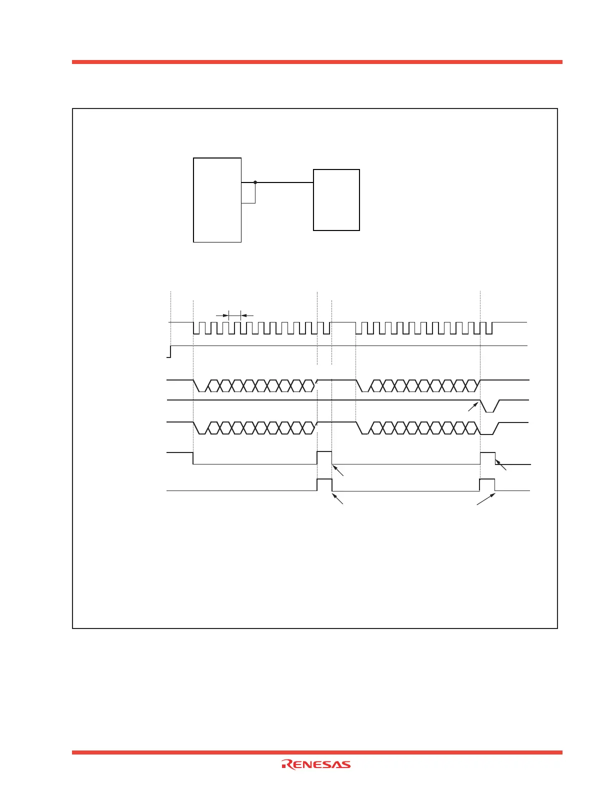
Figure 2.71: Operation of reception in UART mode (compliant with SIM interface)
Example of wiring
Example of operation
Microcomputer
SIM card
TxD
2
RxD
2
Receive enable
bit
(RE)
Receive
complete flag
(RI)
D0
D1 D2
D3
D4 D5
D6
D7ST
P
Start
bit
Parity
bit
TXD2 (Note)
“0”
“1”
“0”
“1”
Receive interrupt
request bit
(IR)
“0”
“1”
Cleared to “0” when interrupt request is accepted, or cleared by software
D0
D1 D2
D3
D4 D5
D6
D7ST
P
SP
Tc
Transfer clock
Since a parity error occurred, the
“L” level returns from TxD
2
RXD2 (Note)
Read to receive buffer
Read to receive buffer
D0
D1 D2
D3
D4 D5
D6
D7ST
P
Signal line level
(Note)
D0
D1 D2
D3
D4 D5
D6
D7ST
P
SP
Note: TxD2 and RxD2 are connected in the manner of wired OR as shown in the connection diagram. So TxD 2 and RxD2 ought to
become the same signal from the logical standpoint, but the output signals turn complex, so they are shown separately. Also,
the signal level resulting from connecting TxD
2 and RxD2 is shown as a signal line level.
(1) Reception enabled
(2) Start reception
(3) Receiving is completed
(4) Data is read
Stop
bit
SP
(5) Parity error occurred
SP
The above timing applies to the following settings :
• Parity is enabled.
• One stop bit.
• Transmit interrupt cause select bit = “1”.
Tc = 16 (n + 1) / fi
fi : value set to BRG2 count source (f1, f8, f32)
Shown in (
) are bit symbols.
n: value set to BRG2
 Loading...


