Clock-Generating Circuit
M30240 Group
Rev.1.00 Sep 24, 2003 Page 23 of 360
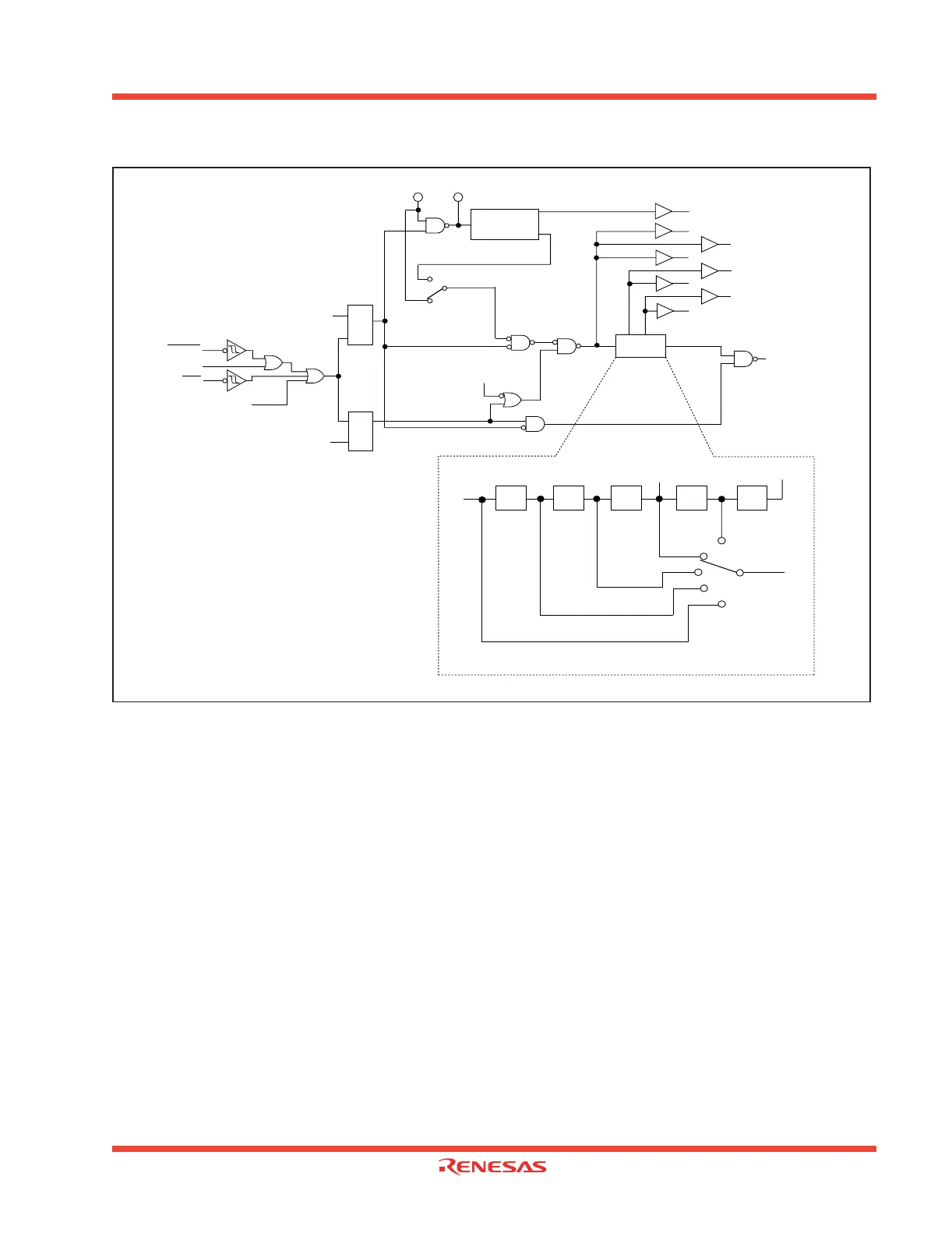
Figure 1.12: Clock-generating circuit
1.2.6.2 Clocks generated by the clock-generating circuit.
Main clock
The main clock is generated by the main clock oscillation circuit. After a reset, the clock is divided by
8 to the internal clock Φ.
After the oscillation of the main clock oscillation circuit has stabilized, the drive capacity of the X
OUT
pin can be reduced using the X
IN
- X
OUT
) drive capacity select bit (bit 5 at address 0007
16
). Reducing
the drive capacity of the X
OUT
pin reduces the power dissipation. This bit defaults to “1” when shifting
to stop mode and after a reset.
Internal clock Φ
The internal clock Φ is the clock that drives the CPU, and is either the main clock or is derived by di-
viding the main clock by 2, 4, 8, or 16. The internal clock Φ is derived by dividing the main clock by 8
after a reset.
When shifting to stop mode, the main clock division select bit (bit 6 at 0006
16
) is set to “1”.
Peripheral Function clock
• f1, f8, f32
The clock for the peripheral devices is derived from the main clock or by dividing it by 8 or 32. The
peripheral function clock is stopped by stopping the main clock or by setting the WAIT peripheral func-
tion clock stop bit (bit 2 at 0006
16
) to “1” and then executing a WAIT instruction.
CM0i : Bit i at address 0006
16
CM1i : Bit i at address 0007
16
FSCCRi: Bit i at address 03DB
16
WAIT instruction
CM02
QS
R
NMI
Interrupt request
level judgment
output
RESET
Software reset
f
AD
Divider
a
d
1/2 1/2 1/2 1/2
CM06=0
CM17,CM16=00
CM06=0
CM17,CM16=01
CM06=0
CM17,CM16=10
CM06=1
CM06=0
CM17,CM16=11
d
a
Details of divider
c
b
b
1/2
c
f
1
f
32
SIO2
f
8
SIO2
f
1
SIO2
f
8
f
32
φ
X
OUT
Main clock
CM10 “1”
Write signal
QS
R
X
IN
Frequency
Synthesizer
Circuit
f
usb (48MHz)
FSCCR0=1
FSCCR0=0
BCLK
fsyn
 Loading...


