Frequency Synthesizer Circuit
M30240 Group
Rev.1.00 Sep 24, 2003 Page 40 of 360
The FSC0 bit in the FSC Control Register enables the frequency synthesizer block. When disabled
(FSC0 = “0”), f
VCO
is held at either a high or low state. When the frequency synthesizer control bit is
active (FSC0 = “1”), a lock status (LS = “1”) indicates that f
SYN
and f
VCO
are the correct frequency. The
LS and FSCO control bits in the FSC Control register are shown in Figure 1.27.
When using the frequency synthesizer, a low-pass filter must be connected to the LPF pin.
Once the frequency synthesizer is enabled, a delay of 2-5ms is recommended before the output of the
frequency synthesizer is used. This is done to allow the output to stabilize. It is also recommended that
none of the registers be modified once the frequency synthesizer is enabled as it will cause the output
to be temporarily (2-5ms) unstable. The MCU clock source is selected via the Frequency Synthesizer
Clock Control register (FSCCR). See Figure 1.28.
Note: None of the registers must be written to once the frequency synthesizer is enabled and used as
the system clock source (FSCCR register, address 03DB
16
, bit “0” set to “1”) because it will cause the
output of the PLL to freeze. Switch system back to f(X
IN) and disable before modifying PLL registers.
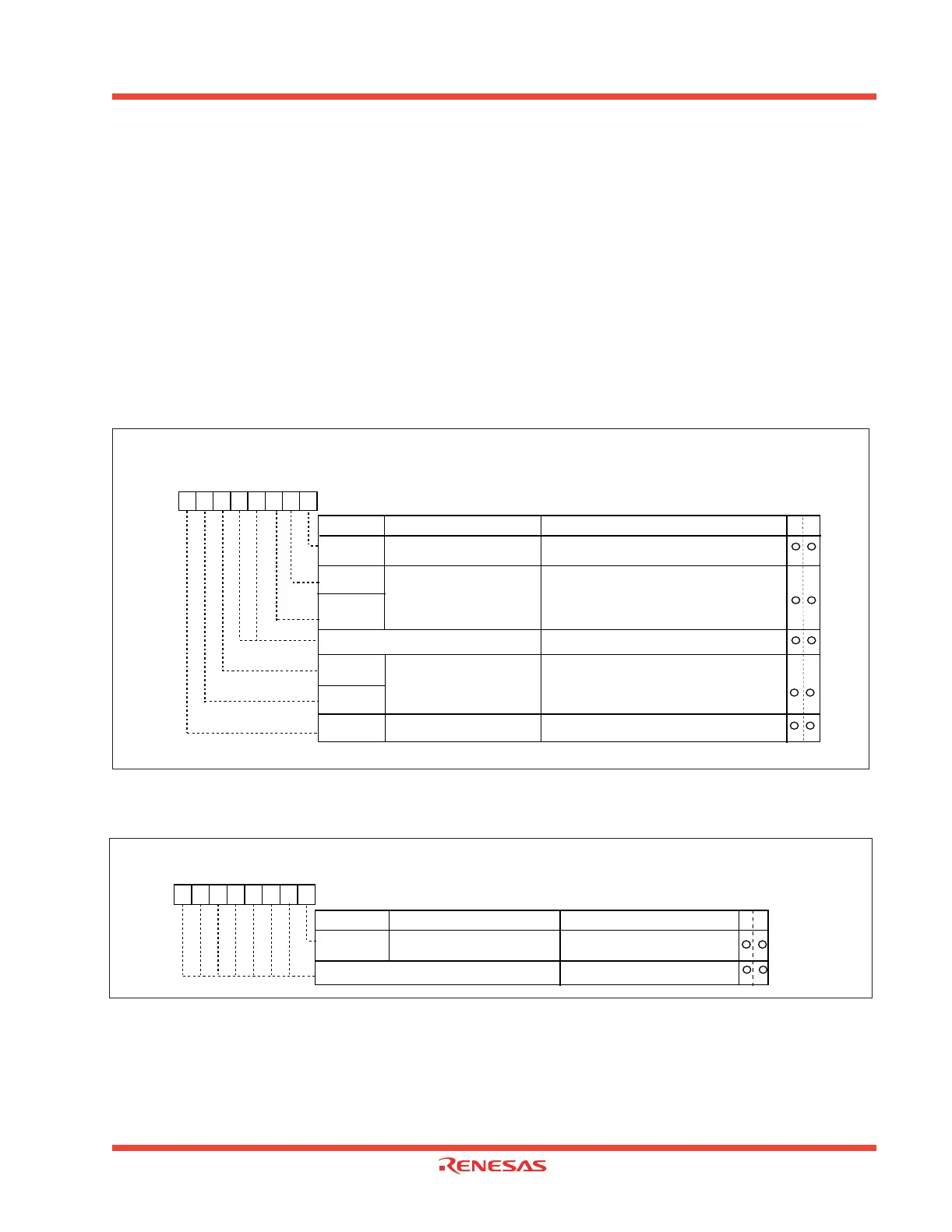
Figure 1.27: Frequency Synthesizer Control Register (FSC)
Figure 1.28: Frequency Synthesizer Clock Control Register (FSCCR)
Frequency Synthesizer Control Register
Symbol Address When reset
FSC 03DC
16
60
16
Bit nameBit symbol
b7 b6 b5 b4 b3 b2 b1 b0
0 : Disable
1 : Enabled
VCO0
FSE
VCO Gain Control
Function
Bit 2 Bit 1
0 0: Lowest Gain (Note)
0 1: Low Gain
1 0: High Gain
1 1: Highest Gain
Frequency Synthesizer Enable
W
R
Reserved bit
Must always be set to "0"
VCO1
CHG0
CHG1
LPF Current Control
Bit 6 Bit 5
0 0: Disabled
0 1: Low Current
1 0: Intermediate Current (Note)
1 1: High Current
LS
Frequency Synthesizer
Lock Status
0: Unlocked
1: Locked
Note :
Recommended
0
0
Frequency Synthesizer Clock Control Register
Symbol Address When reset
FSCCR 03DB
16
00
16
Bit nameBit symbol
b7 b6 b5 b4 b3 b2 b1 b0
0 : X
IN
1 : fsyn
FSCCR0
Function
WR
Reserved
Must always be set to "0"
Clock source selection
0
0
0
0
0
0
0
 Loading...


