SN32F260 Series
32-Bit Cortex-M0 Micro-Controller
SONiX TECHNOLOGY CO., LTD Page 129 Version 1.5
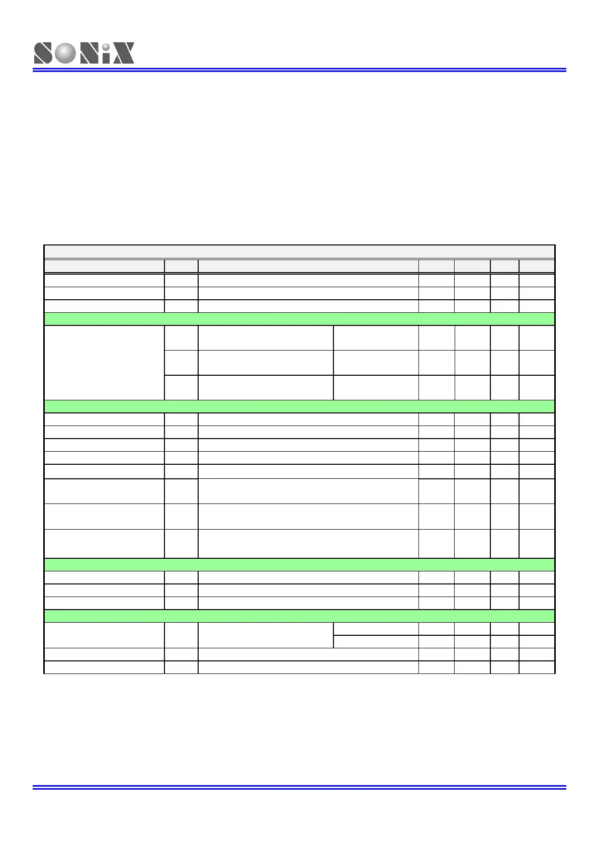
ELECTRICAL CHARACTERISTIC
14.1 ABSOLUTE MAXIMUM RATING
Supply voltage (Vdd)…………………………………………………………………………………………………………………….……………… - 0.3V ~ 5.5V
Input in voltage (Vin)…………………………………………………………………………………………………………………….… Vss – 0.2V ~ Vdd + 0.2V
Operating ambient temperature (Topr)………………………………………...……………………………..……...…………. ………………… -40C ~ + 85C
Storage ambient temperature (Tstor) ………………………………………………………………….………………………………………… –40C ~ + 125C
14.2 ELECTRICAL CHARACTERISTIC
All of voltages refer to Vss, Typical Vdd = 5.0V, Fosc = 12MHz, ambient temperature is 25℃ unless otherwise note.
Supply voltage for core and external rail
VDD rise rate to ensure internal power-on reset
System clock = 48MHz
[1][2[3]
System clock = 32KHz
[1][3][4]
I/O port pull-up resistor
I/O port pull-down resistor
(SWD pull-down pin)
I/O High-level output source
current
I/O Low-level output sink current
3.3V Regulator Output voltage
VCC ≧ 3.60V, IVREG33 >= 60 mA
T=-25℃, Vdd=5V, USB function ON
* Parameters with star mark are non-verified design reference.
[1] IDD measurements were performed with all pins configured as GPIO outputs driven LOW and pull-up resistors disabled and VDD=5V.
[2] IHRC and ILRC are enabled.
[3] LVD and GPIO peripherals are enabled.
[4] IHRC is disabled, ILRC is enabled.
[5] All oscillators and analog blocks are turned off.