SN32F260 Series
32-Bit Cortex-M0 Micro-Controller
SONiX TECHNOLOGY CO., LTD Page 89 Version 1.5
8.4 INTERFACE DESCRIPTION
8.4.1 SPI
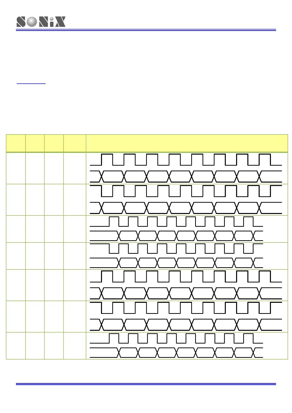
The SPI interface is a 4-wire interface where the SSEL signal behaves as a slave select. The main feature of the SPI
format is that the inactive state and phase of the SCK signal are programmable through the CPOL and CPHA bits in
SPIn_CTRL1 register.
When the “CPOL” clock polarity control bit is LOW, it produces a steady state low value on the SCK pin. If the CPOL
clock polarity control bit is HIGH, a steady state high value is placed on the CLK pin when data is not being transferred.
The “CPHA” clock phase bit controls the phase of the clock on which data is sampled. When CPHA=1, the SCK first
edge is for data transition, and receive and transmit data is at SCK 2
nd
edge. When CPHA=0, the 1
st
bit is fixed already,
and the SCK first edge is to receive and transmit data.
The SPI data transfer timing as following figure:
MSB ... ... ... ... ... bit1 LSB
MSB ... ... ... ... ... bit1 LSB
MSB ... ... ... ... ... bit1 LSB Next data
MSB ... ... ... ... ... bit1 LSB Next data
LSB bit1 ... ... ... ... ... MSB
LSB bit1 ... ... ... ... ... MSB
Next dataLSB bit1 ... ... ... ... ... MSB