112
13 Options
112
Options
Chapter
13
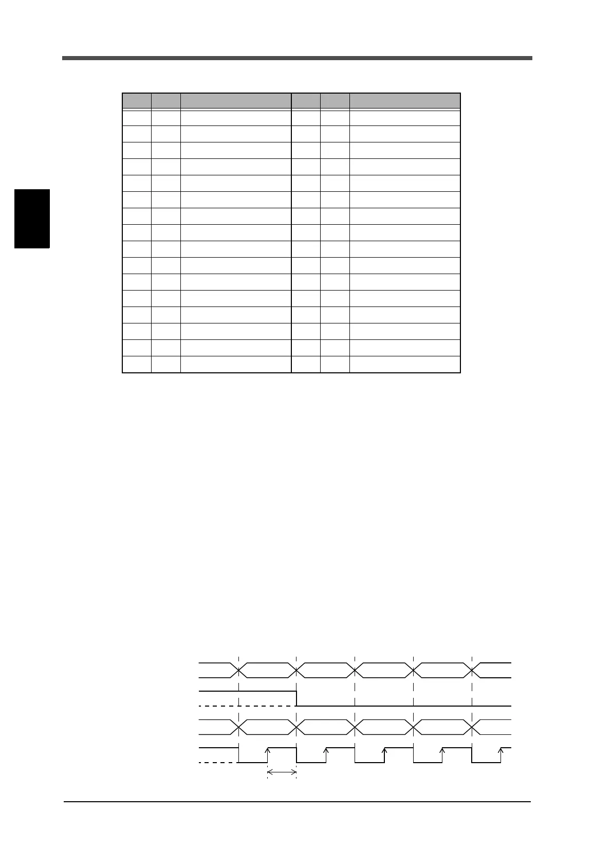
■Connector pin assignment
Compatible connector:
FCN-361J032-AU (manufactured by FUJITSU COMPONENT or equivalent)
Connector cover: FCN-360C032-B (manufactured by FUJITSU COMPONENT or equivalent)
Near zero
Near zero condition is output.
* Only when BCD B9 output selection is set as "1: NZ".
MINUS (polarity)
The polarity of an indicated value being output as BCD data is output.
P. C
P.C is simultaneously output with BCD data at the time of stability.
OVER
OVER is output at the time of over scale (when -LOAD or LOAD, OFL1, OFL2)
STROBE
Strobe pulse is output linked with BCD data. Use a rising edge of pulse (1 -> 0) for reading data.
BCD data update rate can be changed by setting.
No. Signal No. Signal
A1 * COM B1 * COM
A2 Out 1 B2 Out 1000
A3 Out 2 B3 Out 2000
A4 Out 4 B4 Out 4000
A5 Out 8 B5 Out 8000
A6 Out 10 B6 Out 10000
A7 Out 20 B7 Out 20000
A8 Out 40 B8 Out 40000
A9 Out 80 B9 Out 80000/NZ
A10 Out 100 B10 Out MINUS (polarity)
A11 Out 200 B11 Out OVER
A12 Out 400 B12 Out P.C (stable)
A13 Out 800 B13 Out STROBE
A14 In BCD data hold B14 In Logic selection
A15 N.C. B15 N.C.
A16 N.C. B16 N.C.
BCD data
OVER
Strobe range (duty 50%)
STROBE
0
1
0
1
P. C
 Loading...