3.4 Programming Mode
3-32
LED monitor Item Description
4_17
PG pulse rate
(A/B phase signal from
the slave PG)
Shows the pulse rate (kp/s) of the A/B phase signal fed back from the
slave PG. (Shows 1.00 with 1000 p/s.)
4_18
PG pulse rate
(Z phase signal from the
slave PG)
Shows the pulse rate (p/s) of the Z phase signal fed back from the slave
PG.
4_19
(Not used.) ―
4_20
Input voltage on terminal
[32]
Shows the input voltage on terminal [32] on the analog interface card
(option) in volts (V).
4_21
Input current on terminal
[C2]
Shows the input current on terminal [C2] on the analog interface card
(option) in milliamperes (mA).
4_22
Output voltage on
terminal [AO]
Shows the output voltage on terminal [A0] on the analog interface card
(option) in volts (V).
4_23
Output current on
terminal [CS]
Shows the output current on terminal [CS] on the analog interface card
(option) in milliamperes (mA).
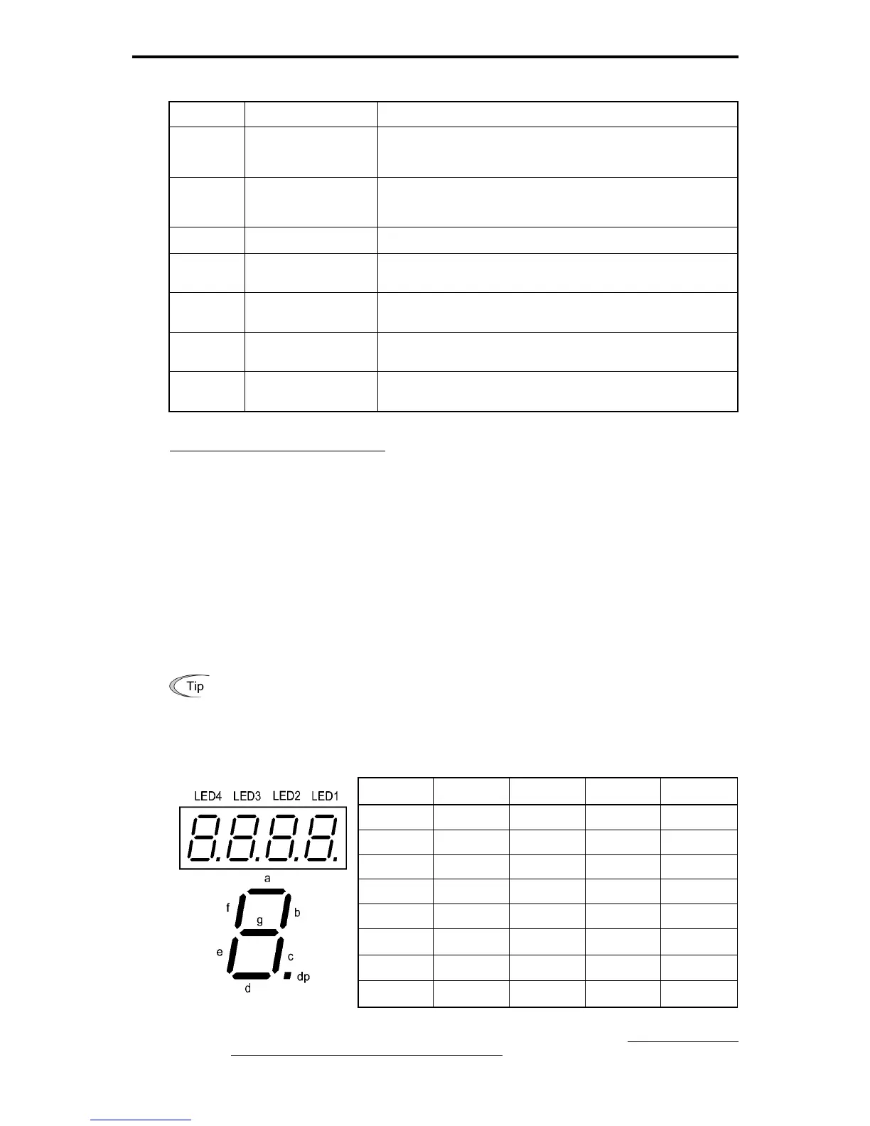
Displaying control I/O signal terminals
The status of control I/O signal terminals may be displayed with ON/OFF of the LED segment or in
hexadecimal.
z
Displaying the I/O signal status with ON/OFF of each LED segment
As shown in Table 3.4-10 and the figure below, each of segment "a" to "dp" on LED1 and LED2 lights
when the corresponding digital input terminal circuit ([FWD], [REV], [X1] to [X9]) is closed; it goes OFF
when it is open. Each of segment "a" to "e" on LED3 lights when the circuit between output terminal [Y1],
[Y2], [Y3] or [Y4] and terminal [CMY] or between terminals [Y5A] and [Y5C] is closed, respectively; it goes
OFF when the circuit is open. Segment "a" on LED4 is for terminals [30A/B/C] and lights when the circuit
between terminals [30C] and [30A] is short-circuited (ON) and goes OFF when it is open.
If all terminal signals are OFF (open), segments "g" on all of LED1 to LED4 will light ("– – – –").
The segment display below indicates the ON/OFF status of the terminals, not the active/inactive
status of input/output.
Table 3.4-10 Segment Display for External Signal Information
Segment
LED4 LED3 LED2 LED1
a 30A/B/C Y1-CMY X7 FWD
b ― Y2-CMY X8 REV
c ― Y3-CMY X9 X1
d ― Y4-CMY ― X2
e ― Y5A-Y5C ― X3
f ― ―
(XF)
*
X4
g ― ―
(XR)
*
X5
dp ― ―
(RST)
*
X6
–: No corresponding control circuit terminal exists.
* (XF), (XR), and (RST) are assigned for communications control. Refer to "Displaying control
I/O signal terminals under communications control" on the next page.
 Loading...