11.2.2 When Using Pulse Output Function (FP-X Compatible Instruction
Mode)
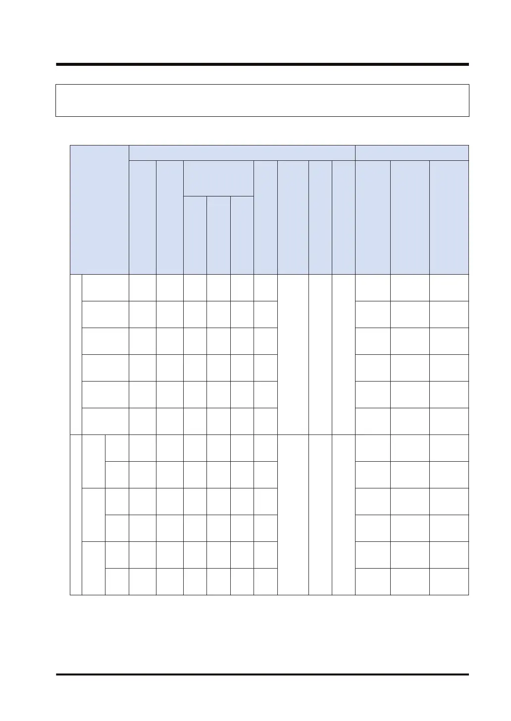
■
Control Unit (transistor output type)
Channel no.
Input / output contact number used Memory area used
CW
or
Pulse
outp
ut
CCW
or
Sign
outp
ut
Deviation
counter
clear output
Ho
me
inpu
t
(Note
1)
Near
home
input
(Note 2)
Ove
r
limit
inpu
t
(Note
3)
J-
poin
t
posi
tioni
ng
start
inpu
t
(Note
4)
BUSY
flag
(Contro
l active
flag)
Elapsed
value
area
(Note 5)
Target
value
area
C14 C30 C60
Independent
CH0 Y0 Y1 Y4 Y8 YC X4
DT
90052
bit4
- -
R911C
DT90348
DT90349
DT90350
DT90351
CH1 Y2 Y3 Y5 Y9 YD X5 R911D
DT90352
DT90353
DT90354
DT90355
CH2 Y4 Y5 - YA Y10 X6 R911E
DT90356
DT90357
DT90358
DT90359
CH3 Y6 Y7 - YB Y11 X7 R911F
DT90360
DT90361
DT90362
DT90363
CH4 Y8 Y9 - - Y12 X2 R9120
DT90364
DT90365
DT90366
DT90367
CH5 YA YB - - Y13 X3 R9121
DT90368
DT90369
DT90370
DT90371
Linear interpolation
(Note 1)
CH0
X-
axis
Y0 Y1 Y4 Y8 YC X4
DT
90052
bit4
- -
R911C
DT90348
DT90349
DT90350
DT90351
Y-
axis
Y2 Y3 Y5 Y9 YD X5 R911D
DT90352
DT90353
DT90354
DT90355
CH2
X-
axis
Y4 Y5 - YA Y10 X6 R911E
DT90356
DT90357
DT90358
DT90359
Y-
axis
Y6 Y7 - YB Y11 X7 R911F
DT90360
DT90361
DT90362
DT90363
CH4
X-
axis
Y8 Y9 - - Y12 X2 R9120
DT90364
DT90365
DT90366
DT90367
Y-
axis
YA YB - - Y13 X3 R9121
DT90368
DT90369
DT90370
DT90371
(Note 1) Even when setting the linear interpolation, the interpolation operation is not performed for the home
return. Execute the operation for X axes and Y axes separately.
(Note 2) The near home input will be valid when an arbitrary input is allocated and the bit 4 of the special data
register DT90052 turns ON.
11.2 Allocation of Memory Areas
WUME-FPXHPOSG-01 11-7
 Loading...