■
Allocation of I/O signals
Signal name
I/O No.
CH0 CH1 CH2 CH3
When using the
transistor output
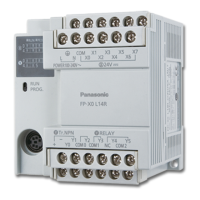
Control Unit
PWM output Y0 Y2 Y4 Y6
Control active
flag (BUSY)
R911C R911D R911E R911F
When using the
relay output type
pulse I/O cassette
PWM output Y100 Y200 - -
Control active
flag (BUSY)
R911C R911D - -
4.1.4 When Using High-speed Counter Function
● The following reserved areas are allocated to the hardware reset input or control active flag.
■
Allocation of I/O signals (When using internal input)
Signal name
I/O No.
CH0 CH1 CH2 CH3 CH4 CH5 CH6 CH7
Count input
Single-phase
input
X0 X1 X2 X3 X4 X5 X6 X7
2-phase input X0 / X1 - X2 / X3 - X4 / X5 - X6 / X7 -
Hardware reset
input
Single-phase
input
X6 - X7 - - - - -
2-phase input X6 - X7 - - - - -
Control active flag
(BUSY)
Single-phase
input
R9110 R9111 R9112 R9113 R9114 R9115 R9116 R9117
2-phase input R9110 - R9112 - R9114 - R9116 -
■
Allocation of I/O signals (When using the input section of the pulse I/O cassette)
Signal name
I/O No.
CH8 CH9 CHA CHB
Count input
Single-phase
input
X100 X101 X200 X201
2-phase input X100 / X101 - X200 / X201 -
Hardware reset
input
Single-phase
input
X102 X102 X202 X202
2-phase input X102 X102 X202 X202
Control active flag
(BUSY)
Single-phase
input
R9118 R9119 R911A R911B
2-phase input R9118 - R911A -
(Note 1) The input X102 can be set to either CH8 or CH9 and the input X202 can be set to either CHA or CHB
as a hardware reset input.
4.1 Confirming I/O Allocation
4-6 WUME-FPXHPOSG-01
 Loading...