12. Timer A
puorG92/C61M
page 115
854fo7002,03.raM21.1.veR
2110-1010B90JER
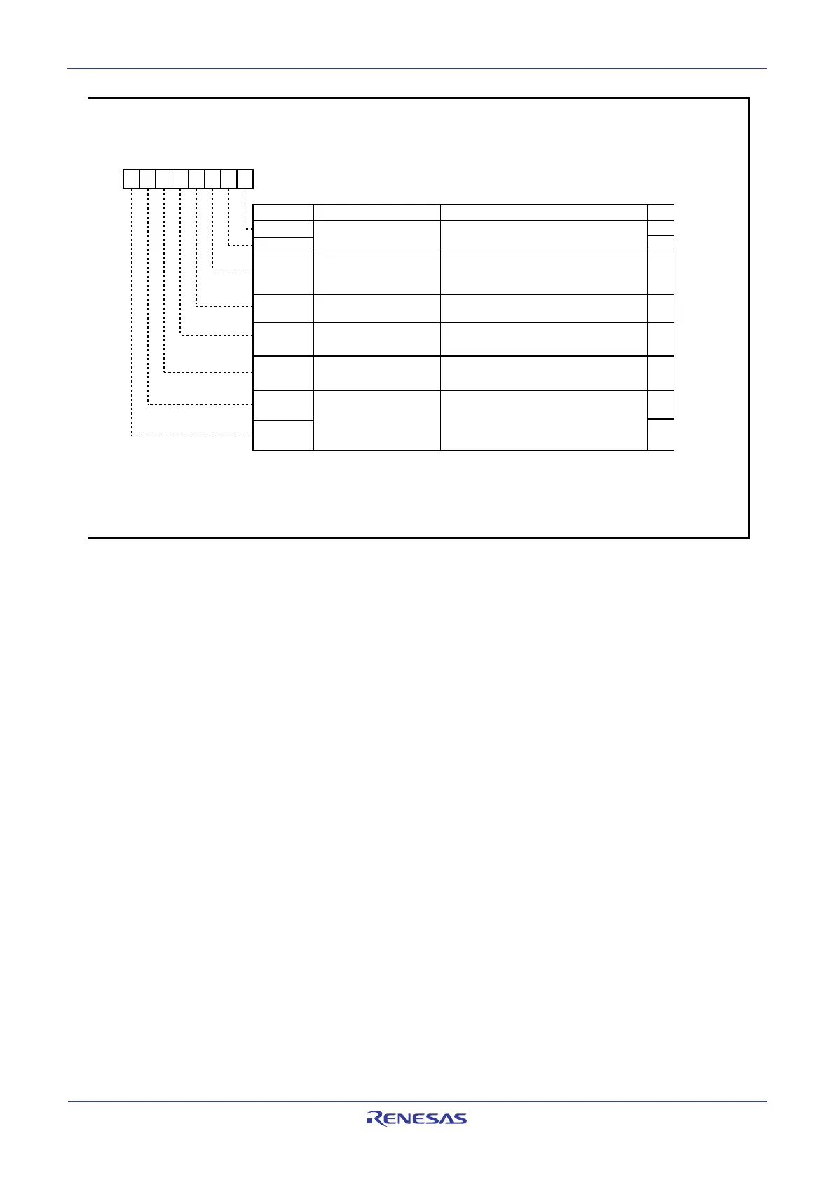
Figure 12.12 TAiMR Register in Pulse Width Modulation Mode
Bit Name
Timer Ai Mode Register (i= 0 to 4)
Symbol
Address
After Reset
TA0MR to TA4MR 0396
16
to 039A
16
00
16
FunctionBit Symbol
b7 b6 b5 b4 b3 b2 b1 b0
b1 b0
1 1: PWM mode
TMOD1
TMOD0
MR0
MR2
MR1
MR3
TCK1
TCK0
Count source select bit
RW
11
0: Functions as a 16-bit pulse width modulator
1: Functions as an 8-bit pulse width modulator
Trigger select bit
External trigger select bit
(1)
RW
RW
RW
RW
RW
RW
RW
RW
0: Write 1 to TAiS bit in the TASF register
1: Selected by bits TAiTGH to TAiTGL
NOTES:
1. Effective when bits TAiTGH and TAiTGL in the ONSF or TRGSR register are 00
2 (TAiIN pin input).
2. The port direction bit for the TAi
IN pin must be set to 0 ( input mode).
16/8-bit PWM mode
select bit
Pulse output funcion
select bit
Operation mode select bit
0: Falling edge of input signal to TAiIN pin
(2)
1: Rising edge of input signal to TAiIN pin
(2)
b7 b6
0 0: f
1
or f
2
0 1: f
8
1 0: f
32
1 1: f
C32
0: Pulse is not output (TAiOUT pin functions as I/O
port)
1: Pulse is output (TAiOUT pin functions as a pulse
output pin)
 Loading...


