13. Timer S
puorG92/C61M
page 167
854fo7002,03.raM21.1.veR
2110-1010B90JER
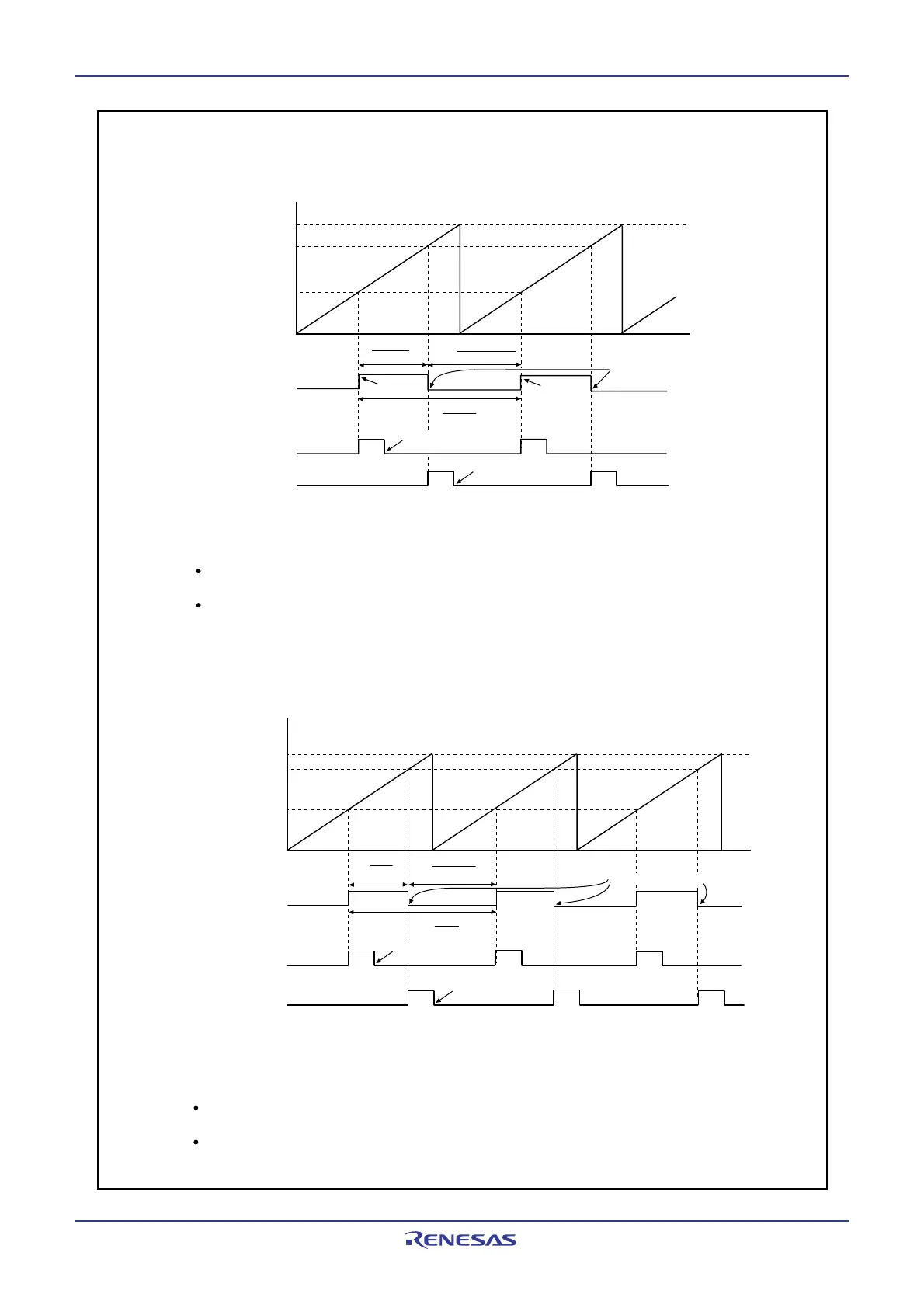
Figure 13.24 Set/Reset Waveform Output Mode
FFFF
16
m
n
n-m
f
BT1
65536
f
BT1
0000
16
FFFF
16
m
p+2
n
0000
16
65536-n+m
f
BT1
n-m
f
BT1
p+2-n+m
f
BT1
p+2
f
BT1
(1) Free-running operation
(Bits RST2 and RST1 in the G1BCR0 register and the RST4 bit in the G1BCR1
register are set to 0)
j=0, 2, 4, 6 k=j+1
m : Setting value of the G1POj register n: Setting value of the G1POk register
G1IRj, G1IRk bits: Bits in the G1IR register
Inverse
Write 0 by program
if setting to 0
Inverse
(2) Base timer is reset when the base timer matches either following register
(a) G1PO0 (enabled by setting bit RST1 to 1, and bits RST4 and RST2 to 0), or
(b) G1BTRR (enabled by setting bit RST4 to 1, and bits RST2 and RST1 to 0)
j=2, 4, 6 k=j+1
m : Setting value of the G1POj register n: Setting value of the G1POk register
p: Setting value of either register G1PO0 or G1BTRR
G1IRj, G1IRk bits: Bits in the G1IR register
Return to default
output level
inverse
Return to default output level
Write 0 by program
if setting to 0
When setting to 0,
write 0 by program
Base timer
OUTC1j pin
G1IRj bit
G1IRk bit
Base timer
OUTC1j pin
G1IRj bit
G1IRk bit
The above applies under the following conditions.
The IVL bit in the G1POCRj register is set to 0 (L output as a default value). The INV bit is set to 0 (not
inversed).
Bits UD1 and UD0 are set to 00
2 (counter increment mode).
The above applies under the following conditions.
The IVL bit in the G1POCRj register is set to 0 (L output as a default value). The INV bit is set to 0
(not inversed).
Bits UD1 and UD0 are set to 00
2 (counter increment mode).
 Loading...


