14.Serial I/O
puorG92/C61M
page 192
854fo7002,03.raM21.1.veR
2110-1010B90JER
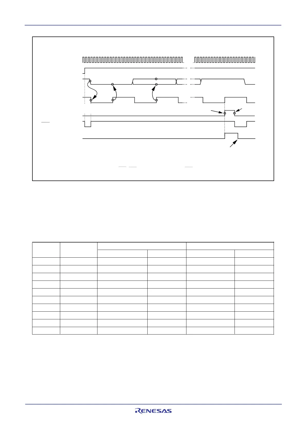
• Example of receive timing when transfer data is 8 bits long (parity disabled, one stop bit)
Figure 14.17 Receive Operation
D0
Start
bit
Sampled “L”
UiBRG count
source
RxDi
Transfer clock
RTSi
Stop bit
1
0
0
1
“H”
“L”
0
1
Reception triggered when transfer clock
is generated by falling edge of start bit
UiC1 register
RE bit
UiC1 register
RI bit
SiRIC register
IR bit
Cleared to 0 when interrupt request is accepted, or cleared to 0 by program
Receive data taken in
D7
D1
Transferred from UARTi receive
register to UiRB register
The above timing diagram applies to the case where the register bits are set as follows:
• Set the PRYE bit in the UiMR register to 0 (parity disabled)
• Set the STPS bit in the UiMR register to 0 (1 stop bit)
• Set the CRD bit in the UiC0 register to 0 (CTSi/RTSi enabled), the CRS bit to 1 (RTSi selected)
i = 0 to 2
Read out from
UiRB register
14.1.2.1 Bit Rates
In UART mode, the frequency set by the UiBRG register (i=0 to 2) divided by 16 become the bit rates.
Table 14.9 lists example of bit rate and settings.
Table 14.9 Example of Bit Rates and Settings
Bit Rate Count Source Peripheral Function Clock : 16MHz Peripheral Function Clock : 20MHz
(bps) of BRG
Set Value of BRG : n Actual Time (bps) Set Value of BRG : n Actual Time (bps)
1200 f8 103(67h) 1202 129(81h) 1202
2400 f8 51(33h) 2404 64(40h) 2404
4800 f8 25(19h) 4808 32(20h) 4735
9600 f1 103(67h) 9615 129(81h) 9615
14400 f1 68(44h) 14493 86(56h) 14368
19200 f1 51(33h) 19231 64(40h) 19231
28800 f1 34(22h) 28571 42(2Ah) 29070
31250 f1 31(1Fh) 31250 39(27h) 31250
38400 f1 25(19h) 38462 32(20h) 37879
51200 f1 19(13h) 50000 24(18h) 50000
 Loading...


