14. Serial I/O
puorG92/C61M
page 193
854fo7002,03.raM21.1.veR
2110-1010B90JER
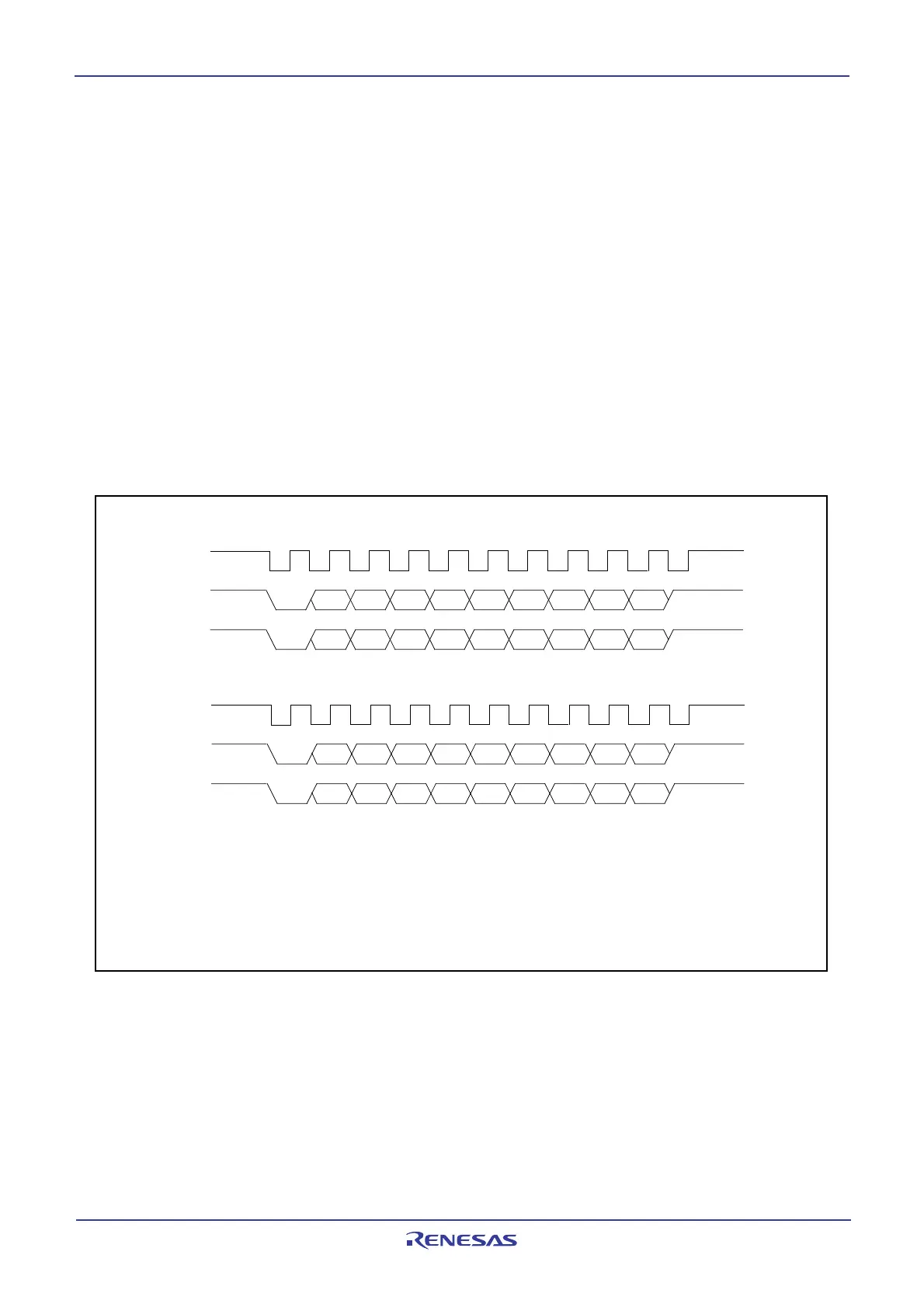
(1) When the UFORM bit in the UiC0 register is set to 0 (LSB first)
(2) When the UFORM bit in the UiC0 register is set to 1 (MSB first)
NOTE:
1. This applies to the case where the CKPOL bit in the UiC0 register is set to 0 (transmit data output at the
falling edge and the receive data taken in at the rising edge of the transfer clock), the UiLCH bit in the UiC1
register is set to 0 (no reverse), the STPS bit in the UiMR register is set to 0 (1 stop bit) and the PRYE bit in
the UiMR register is set to 1 (parity enabled).
D1 D2 D3 D4 D5 D6 SPD0
D1 D2 D3 D4 D5 D6 SPD0
TXDi
RXDi
CLKi
D6 D5 D4 D3 D2 D1 D0
D7
TXDi
RXDi
CLKi
ST
ST
D7 P
D7 P
SP
SP
ST
ST
P
P
D6 D5 D4 D3 D2 D1 D0
D7
ST : Start bit
P : Parity bit
SP : Stop bit
i = 0 to 2
14.1.2.2 Counter Measure for Communication Error
If a communication error occurs while transmitting or receiving in UART mode, follow the procedure
below.
• Resetting the UiRB register (i=0 to 2)
(1) Set the RE bit in the UiC1 register to 0 (reception disabled)
(2) Set the RE bit in the UiC1 register to 1 (reception enabled)
• Resetting the UiTB register (i=0 to 2)
(1) Set bits SMD2 to SMD0 in UiMR register 0002 (Serial I/O disabled)
(2) Set bits SMD2 to SMD0 in UiMR register 0012, 1012, 1102
(3) 1 is written to TE bit in the UiC1 register (reception enabled), regardless of the TE bit
14.1.2.3 LSB First/MSB First Select Function
As shown in Figure 14.18, use the UFORM bit in the UiC0 register to select the transfer format. This
function is valid when transfer data is 8 bits long.
Figure 14.18 Transfer Format
 Loading...


