14.Serial I/O
puorG92/C61M
page 194
854fo7002,03.raM21.1.veR
2110-1010B90JER
Transfer clock
“H”
“L”
D0 D1 D2 D3 D4 D5 D6 D7 PSPST
TxD
2
(no reverse)
“H”
“L”
TxD2
(reverse)
SPST D3 D4 D5 D6 D7 PD0 D1 D2
“H”
“L”
(1) When the U2LCH bit in the U2C1 register is set to 0 (no reverse)
(2) When the U2LCH bit in the U2C1 register is set 1 (reverse)
Transfer clock
“H”
“L”
NOTE:
1. This applies to the case where the CKPOL bit in the U2C0 register is set to 0
(transmit data output at the falling edge of the transfer clock), the UFORM bit in
the U2C0 register is set to 0 (LSB first), the STPS bit in the U2MR register is set
to 0 (1 stop bit) and the PRYE bit in the U2MR register is set to 1 (parity
ST: Start bit
P: Parity bit
SP: Stop bit
(1) When the IOPOL bit in the U2MR register is set to 0 (no reverse)
(2) When the IOPOL bit in the U2MR register is set to 1 (reverse)
ST: Start bit
P: Parity bit
SP: Stop bit
D0 D1 D2 D3 D4 D5 D6 D7 PSPST
SPST
D3 D4 D5 D6 D7 PD0 D1 D2
D0 D1 D2 D3 D4 D5 D6 D7
PSPST
“H”
SPST D3 D4 D5 D6 D7 PD0 D1 D2
Transfer clock
TxD
2
(no reverse)
RxD2
(no reverse)
Transfer clock
TxD
2
(reverse)
RxD2
(reverse)
“L”
“H”
“L”
“H”
“L”
“H”
“L”
“H”
“L”
“H”
“L”
NOTE:
1. This applies to the case where the UFORM bit in the U2C0 register is set
to 0 (LSB first), the STPS bit in the U2MR register is set to 0 (1 stop bit)
and the PRYE bit in the U2MR register is set to 1 (parity enabled).
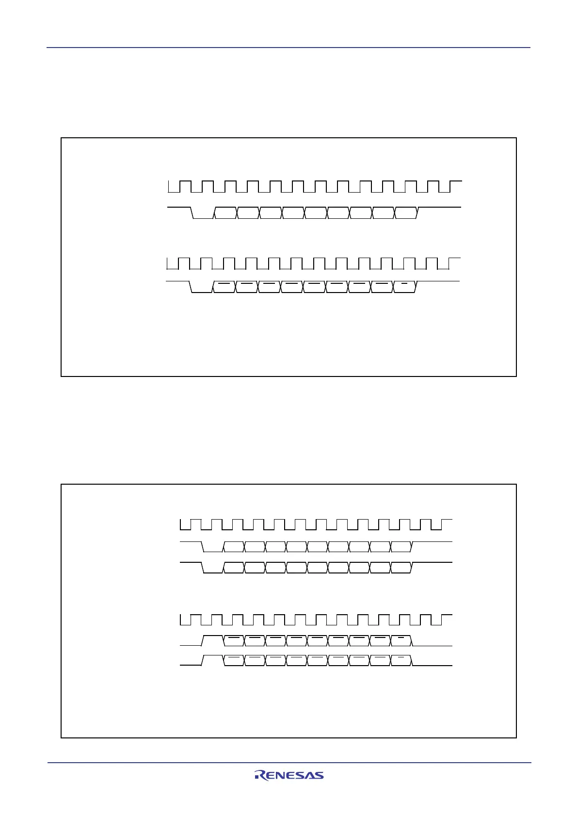
14.1.2.4 Serial Data Logic Switching Function (UART2)
The data written to the U2TB register has its logic reversed before being transmitted. Similarly, the
received data has its logic reversed when read from the U2RB register. Figure 14.19 shows serial
data logic.
Figure 14.19 Serial Data Logic Switching
14.1.2.5 TxD and RxD I/O Polarity Inverse Function (UART2)
This function inverses the polarities of the TXD2 pin output and RXD2 pin input. The logic levels of all
input/output data (including the start, stop and parity bits) are inversed. Figure 14.20 shows the TXD
pin output and RXD pin input polarity inverse.
Figure 14.20 TXD and RXD I/O Polarity Inverse
 Loading...


