14. Serial I/O
puorG92/C61M
page 208
854fo7002,03.raM21.1.veR
2110-1010B90JER
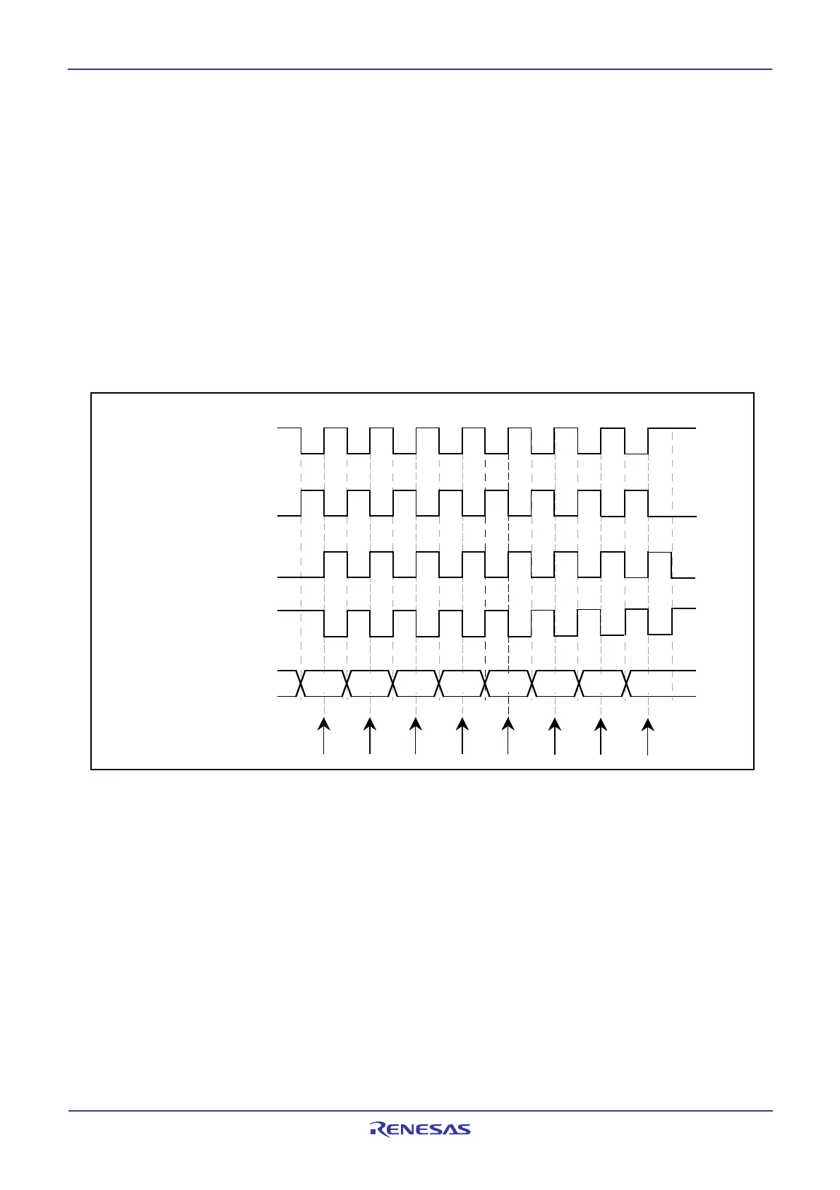
14.1.4.1 Clock Phase Setting Function
One of four combinations of transfer clock phases and polarities can be selected using the CKPH bit
in the U2SMR3 register and the CKPOL bit in the U2C0 register.
Make sure the transfer clock polarity and phase are the same for the master and slave to communi-
cate.
14.1.4.1.1 Master (Internal Clock)
Figure 14.27 shows the transmission and reception timing in master (internal clock).
14.1.4.1.2 Slave (External Clock)
Figure 14.28 shows the transmission and reception timing (CKPH=0) in slave (external clock) while
Figure 14.29 shows the transmission and reception timing (CKPH=1) in slave (external clock).
Figure 14.27 Transmission and Reception Timing in Master Mode (Internal Clock)
D
a
t
a
o
u
t
p
u
t
t
i
m
i
n
g
D
a
t
a
i
n
p
u
t
t
i
m
i
n
g
D0 D1 D2 D3 D4 D6 D7D5
C
l
o
c
k
o
u
t
p
u
t
(
C
K
P
O
L
=
0
,
C
K
P
H
=
0
)
"
H
"
"
L
"
C
l
o
c
k
o
u
t
p
u
t
(
C
K
P
O
L
=
1
,
C
K
P
H
=
0
)
"
H
"
"
L
"
C
l
o
c
k
o
u
t
p
u
t
(
C
K
P
O
L
=
0
,
C
K
P
H
=
1
)
"
H
"
"
L
"
Clock output
(CKPOL=1, CKPH=
1)
"H"
"
L
"
"H"
"L
"
 Loading...


