15. A/D Converter
puorG92/C61M
page 246
854fo7002,03.raM21.1.veR
2110-1010B90JER
Figure 15.23 ADTRGCON Register in Delayed Trigger Mode 0
Table 15.11 Trigger Select Bit Setting in Delayed Trigger Mode 0
Trigger
Timer B0, B1 underflow
TRG
0
HPTRG0
1
TRG1
0
HPTRG1
1
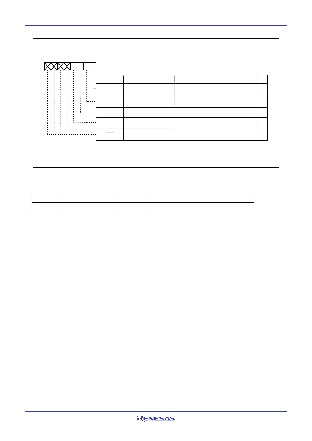
A/D Trigger Control Register
(1)
Symbol Address After Reset
ADTRGCON 03D2
16
00
16
Bit Name FunctionBit Symbol
b7 b6 b5 b4 b3 b2 b1 b0
A/D operation mode select
bit 2
SSE
AN
0
trigger select bit See Table 15.11
HPTRG1 AN
1
trigger select bit
HPTRG0
RW
RW
RW
RW
RW
See Table 15.11
Nothing is assigned. If necessary, set to 0.
When read, the content is 0
(b7-b4)
NOTE:
1. If ADTRGCON is rewritten during A/D conversion, the conversion result will be undefined.
DTE
111
Simultaneous sample sweep mode or
delayed trigger mode 0, 1
A/D operation mode select
bit 3
Delayed trigger mode 0, 1
1
 Loading...


