16. MULTI-MASTER I
2
C bus INTERFACE
puorG92/C61M
page 280
854fo7002,03.raM21.1.veR
2110-1010B90JER
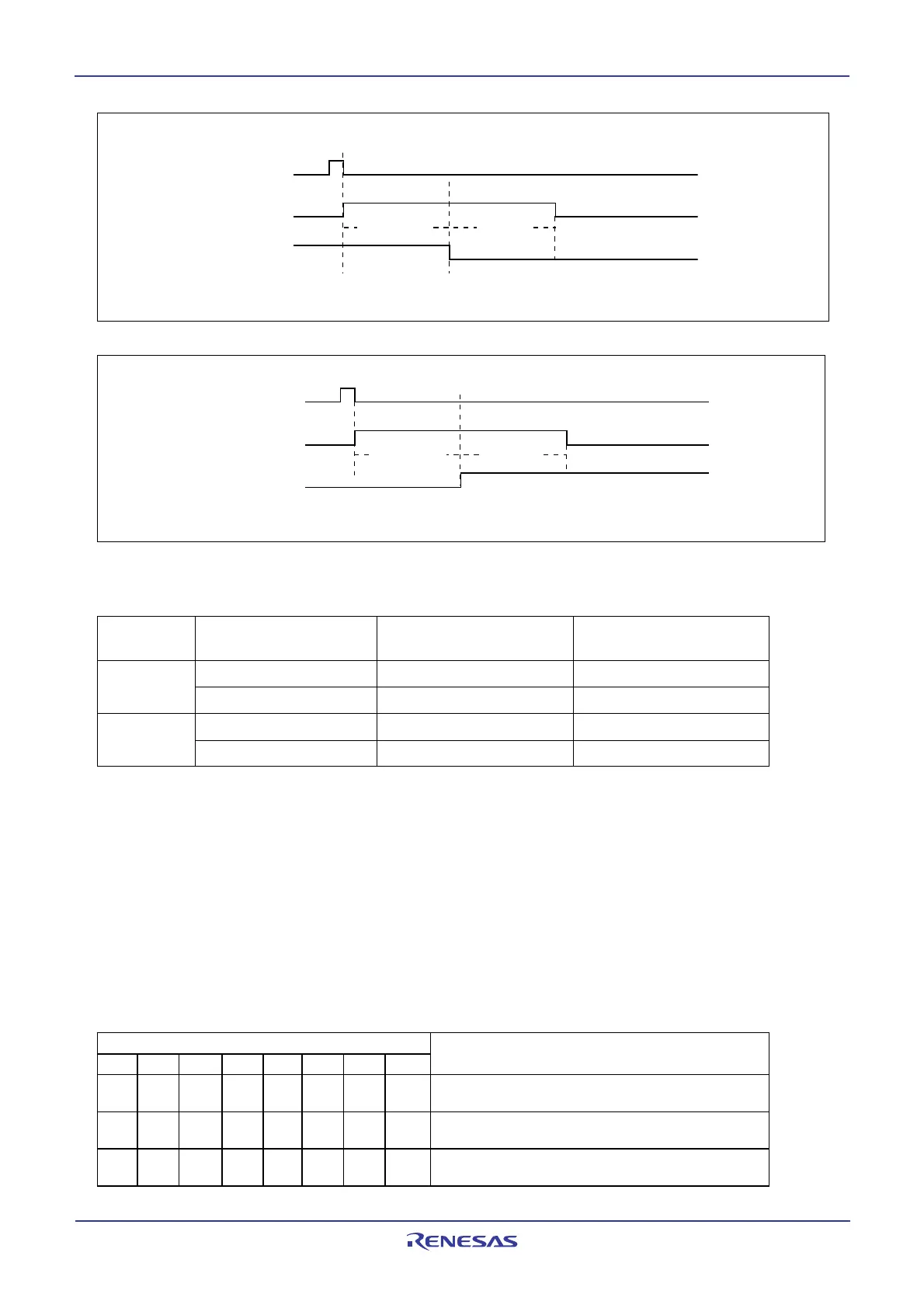
Figure 16.16 Start condition generation timing diagram
Figure 16.17 Stop condition generation timing diagram
Table 16.8 Start/Stop generation timing table
As mentioned above, when bits MST and TRX are set to 1, START condition or STOP condition mode is
entered by writing 1 or 0 to the BB flag in the S10 register and writing 0 to the PIN bit and 4 low-order bits in
the S10 register at the same time. Then SDAMM is left open in the START condition standby mode and
SDAMM is set to low-level ("L") in the STOP condition standby mode. When the S00 register is set, the
START/STOP conditions are generated. In order to set bits MST and TRX to 1 without generating the
START/STOP conditions, write 1 to the 4 low-order bits simultaneously. Table 16.9 lists functions along
with the S10 register settings.
N OTE:
1. Actual time at the time of V
IIC = 4MHz, The contents in () denote cycle numbers.
Table 16.9 S10 Register Settings and Functions
0
0
r
e
g
s
t
e
r
C
L
D
A
Hold
time
S
e
t
u
p
t
i
m
e
00 reg
ster
C
L
DA
Setup
time
H
o
l
d
t
i
m
e
noitidnoCpotS/tratS
tiBtceleSnoitareneG
edoMkcolCdradnatSedoMkcolCdeeps-hgiH
emitputeS
00.5 µ )selcyc02(s5.2 µ )selcyc01(s
10.31 µ )selcyc25(s5.6 µ )selcyc62(s
emitdloH
00.5 µ )selcyc02(s5.2 µ )selcyc01(s
10.31 µ )selcyc25(s5.6 µ )selcyc62(s
sgnitteSretsigeR01S
noitcnuF
TSMXRTBBNIPLASAA0SABRL
11 10000 0
retsamniybdnatsnoitidnocTRATSehtpugnitteS
edomtimsnart
110 0000 0
retsamniybdnatsnoitidnocPOTSehtpugnitteS
edomtimsnart
1/01/0-01111
otrefer(edomnoitacinummochcaepugnitteS 5.61
I
2
retsigersutatsC )
 Loading...


