17. CAN Module
puorG92/C61M
page 290
854fo7002,03.raM21.1.veR
2110-1010B90JER
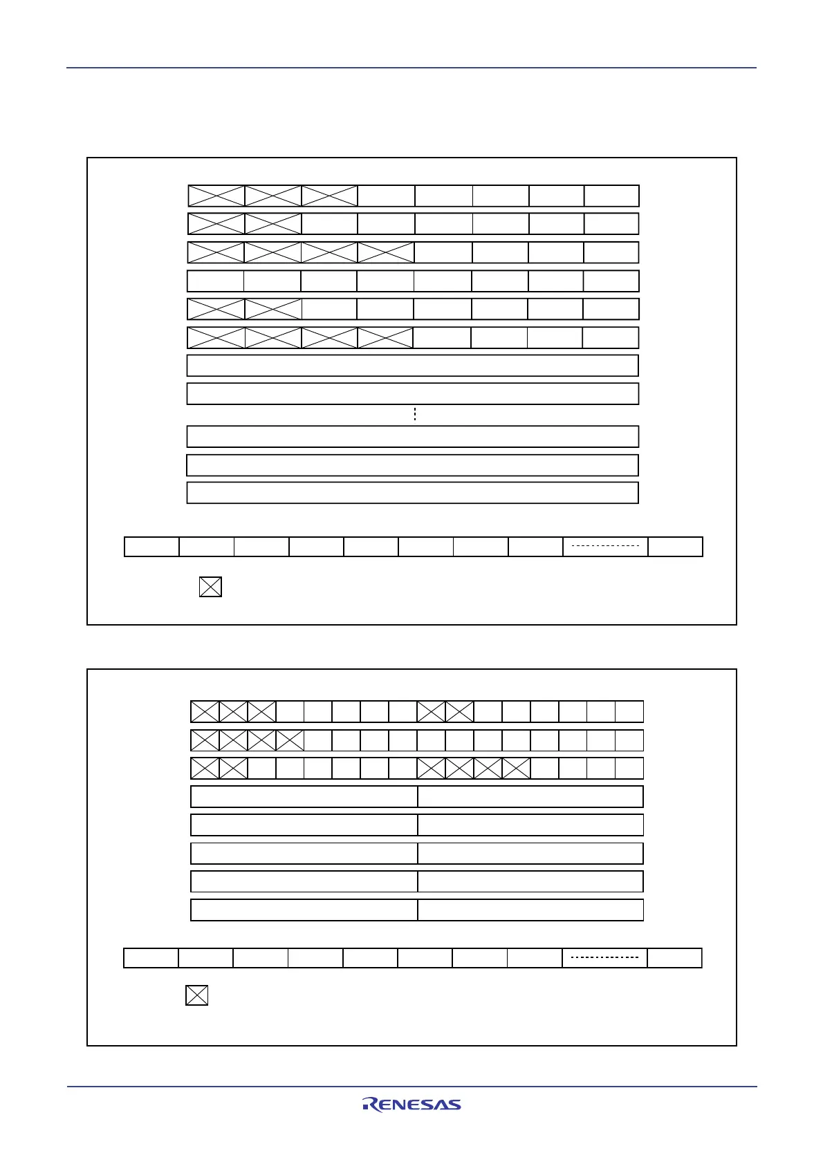
Figures 17.2 and 17.3 show the bit mapping in each slot in byte access and word access. The content of
each slot remains unchanged unless transmission or reception of a new message is performed.
Figure 17.2 Bit Mapping in Byte Access
Figure 17.3 Bit Mapping in Word Access
bit 7 bit 0
SID
10
SID
9
SID
8
SID
7
SID
6
SID
5
SID
4
SID
3
SID
2
SID
1
SID
0
EID
17
EID
16
EID
15
EID
14
EID
13
EID
12
EID
11
EID
10
EID
9
EID
8
EID
7
EID
6
EID
5
EID
4
EID
3
EID
2
EID
1
EID
0
DLC
3
DLC
2
DLC
1
DLC
0
Data Byte 0
Data Byte 1
Data Byte 7
NOTE:
1. When
The value is 0 when read on the reception slot configuration.
is read, the value is the one written upon the transmission slot configuration.
CAN Data Frame:
Time Stamp high-order byte
Time Stamp low-order byte
SID
10 to 6
SID
5 to 0
EID
17 to 14
EID
13 to 6
EID
5 to 0
DLC
3 to 0
Data Byte 0 Data Byte 1 Data Byte 7
bit 15 bit 0
SID
10
SID
9
SID
8
SID
7
SID
6
SID
5
SID
4
SID
3
SID
2
SID
1
SID
0
bit 8 bit 7
EID
17
EID
16
EID
15
EID
14
EID
13
EID
12
EID
11
EID
10
EID
9
EID
8
EID
7
EID
6
EID
5
EID
4
EID
3
EID
2
EID
1
EID
0
DLC
3
DLC
2
DLC
1
DLC
0
Data Byte 0 Data Byte 1
Time Stamp high-order byte Time Stamp low-order byte
CAN Data Frame:
Data Byte 2 Data Byte 3
Data Byte 4
Data Byte 5
Data Byte 6
Data Byte 7
NOTE:
1.
SID
10 to 6
SID
5 to 0
EID
17 to 14
EID
13 to 6
EID
5 to 0
DLC
3 to 0
When
The value is "0" when read on the reception slot configuration.
is read, the value is the one written upon the transmission slot configuration.
Data Byte 0 Data Byte 1 Data Byte 7
 Loading...


