19. Programmable I/O Ports
puorG92/C61M
page 318
854fo7002,03.raM21.1.veR
2110-1010B90JER
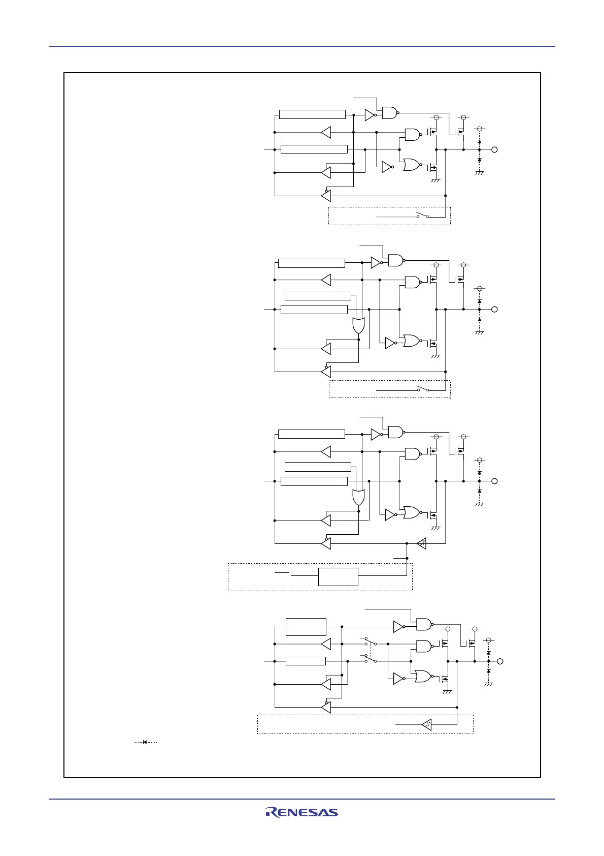
Figure 19.1 I/O Ports (1)
P10 to P13
P15, P16
P22 to P27, P30, P60, P61, P64,
P6
5, P74 to P76, P80, P81
P00 to P07,
P10
0 to P103
P3
0
to P3
7
(inside dotted-line included)
(inside dotted-line not included)
Data bus
Data bus
(1)
Analog input
Pull-up selection
Direction register
Port latch
P1
4
(inside dotted-line not included)
(inside dotted-line included)
P1
7
(inside dotted-line not included)
(inside dotted-line included)
P3
2
(inside dotted-line not included)
(inside dotted-line included)
Data bus
Direction register
Port latch
Pull-up selection
(1)
Port P1 control register
Analog input
Direction register
Port latch
Pull-up selection
(1)
Port P1 control register
Input to respective peripheral functions
Digital
debounce
INPC1
7/INT5
"1"
Output
Data bus
Direction
register
Port latch
Pull-up selection
(1)
Input to respective peripheral functions
NOTE:
1. symbolizes a parasitic diode.
Make sure the input voltage on each port will not exceed Vcc.
 Loading...


