20. Flash Memory Version
puorG92/C61M
page 356
854fo7002,03.raM21.1.veR
2110-1010B90JER
1
2
3
4
5
6
7
8
9
10
11
12
13
14
15
16
21
2
2
23
24
2
5
26
27
2
8
29
30
31
32
33
34
35
36
37
38
39
40
6
0
5
9
58
57
5
6
5
5
54
53
52
51
50
49
48
47
46
45
44
43
42
41
6
4
63
62
61
17
18
19
2
0
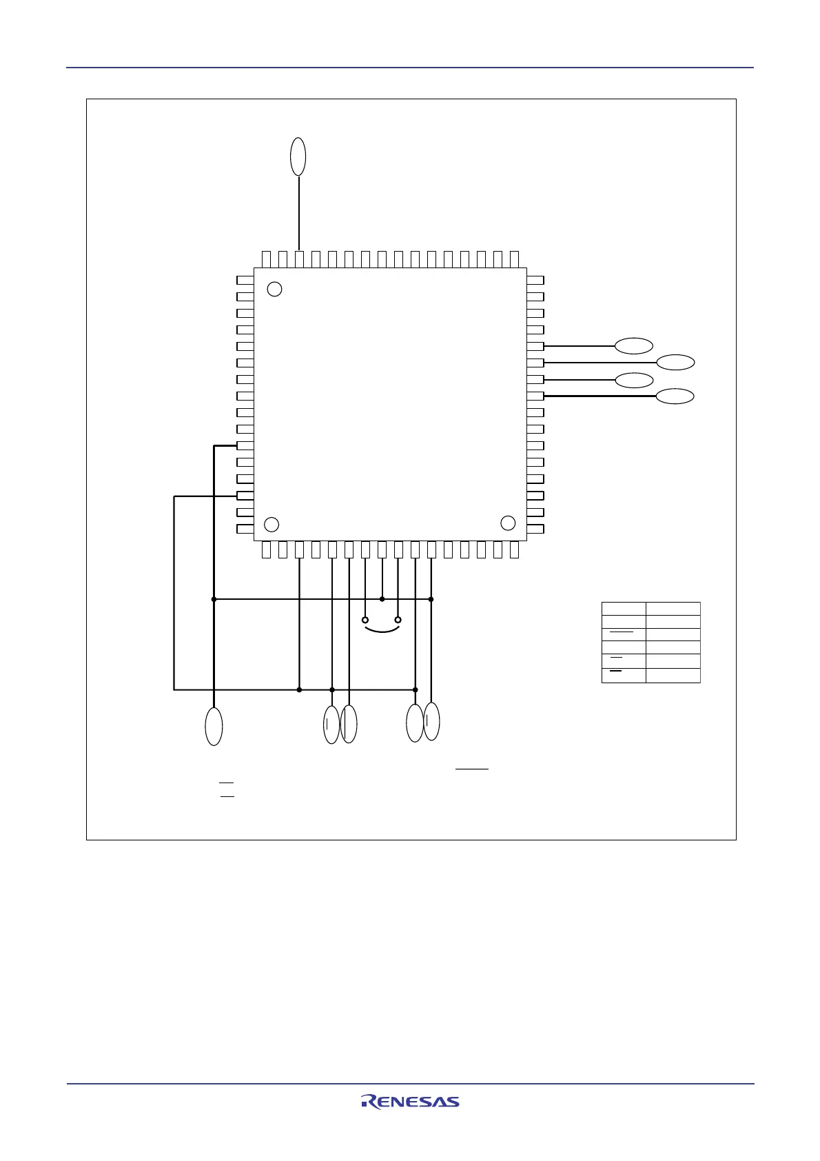
BUSY
SCLK
RxD
TxD
Vcc
Vss
RESET
Connect
oscillator
circuit
CE
(1)
RP
(1)
NOTE:
1. Set the following, either or both, in serial I/O Mode, while the RESET pin is applied a low-level ("L") signal.
-Connect the CE pin to Vcc.
-Connect the RP pin to Vss and the P16 pin to Vcc.
P1
6
(1)
Mode setup method
Signal
CNVss
Reset
P1
6
CE
RP
Value
Vcc
Vss to Vcc
Vcc
(1)
Vcc
(1)
Vss
(1)
M16C/29 Group (64-pin package)
(Flash memory version)
(PLQP0064KB-A (64P6Q-A))
Figure 20.15 Pin Connections for Serial I/O Mode (1)
 Loading...


