1. Overview
puorG92/C61M
page 18
854fo7002,03.raM21.1.veR
2110-1010B90JER
1.5 Pin Description
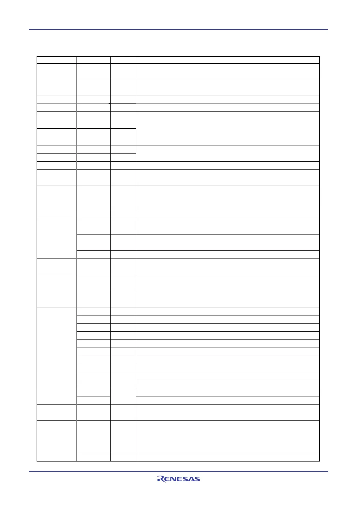
Apply 0V to the Vss pin. Apply following voltage to the Vcc pin.
2.7 to 5.5 V (Normal), 3.0 to 5.5 V (T-ver.), 4.2 to 5.5 V (V-ver.)
Supplies power to the A/D converter. Connect the AV
CC pin to VCC and
the AVSS pin to VSS
___________
The microcomputer is in a reset state when "L" is applied to the RESET pin
Connect the CNVSS pin to VSS
I/O pins for the main clock oscillation circuit. Connect a ceramic resonator
or crystal oscillator between X
IN and XOUT. To apply external clock, apply
it to X
IN and leave XOUT open. If XIN is not used (for external oscillator or
external clock) connect XIN pin to VCC and leave XOUT open
I/O pins for the sub clock oscillation circuit. Connect a crystal oscillator
between XCIN and XCOUT
Outputs the clock having the same frequency as f1, f8, f32, or fC
______ ________
Input pins for the INT interrupt. INT2 can be used for Timer A Z-phase
function
_______ _______
Input pin for the NMI interrupt. NMI cannot be used as I/O port while the three-
_______
phase motor control is enabled. Apply a stable "H" to NMI after setting it's
direction register to "0" when the three-phase motor control is enabled
Input pins for the key input interrupt
I/O pins for the timer A0 to A4
Input pins for the timer A0 to A4
Input pin for Z-phase
Input pins for the timer B0 to B2
Output pins for the three-phase motor control timer
Input and output pins for the three-phase motor control timer
Input pins for data transmission control
Output pins for data reception control
Inputs and outputs the transfer clock
Inputs serial data
Inputs serial data
Outputs serial data
Outputs serial data
Output pin for transfer clock
Inputs and outputs serial data
Inputs and outputs the transfer clock
Inputs and outputs serial data
Inputs and outputs the transfer clock
Applies reference voltage to the A/D converter
Analog input pins for the A/D converter
Input pin for an external A/D trigger
V
CC, VSS
AVCC
AVSS
____________
RESET
CNVSS
XIN
XOUT
XCIN
XCOUT
CLKOUT
________ ________
INT0 to INT5
_______
NMI
_____ _____
KI0 to KI3
TA0OUT to
TA4OUT
TA0IN to
TA4IN
ZP
TB0
IN to
TB2IN
___ ___
U, U, V, V,
___
W, W
IDU, IDW,
_____
IDV, SD
_________ _________
CTS0 to CTS2
_________ _________
RTS0 to RTS2
CLK0 to CLK3
RxD0 to RxD2
SIN3
TxD0 to TxD2
SOUT3
CLKS1
SDA2
SCL2
SDAMM
SCLMM
VREF
AN0 to AN7
AN0
0
to AN0
3
AN2
4
AN3
0
to AN3
2
___________
ADTRG
Power supply
Analog power
supply
Reset input
CNVSS
Main clock
input
Main clock
output
Sub clock input
Sub clock output
Clock output
______
INT interrupt
input
_______
NMI interrupt
input
Key input interrupt
Timer A
Timer B
Three-phase
motor control
timer output
Serial I/O
I
2
C bus Mode
Multi-master
I
2
C bus
Reference
voltage input
A/D converter
I
I
I
I
I
O
I
O
O
I
I
I
I/O
I
I
I
O
I/O
I
O
I/O
I
I
O
O
O
I/O
I/O
I
I
I
I: Input O: Output I/O: Input and output
Classification Symbol I/O Type Function
Table 1.14 Pin Description (64-pin and 80-pin packages)
 Loading...


