6. Processor Mode
puorG92/C61M
page 46
854fo7002,03.raM21.1.veR
2110-1010B90JER
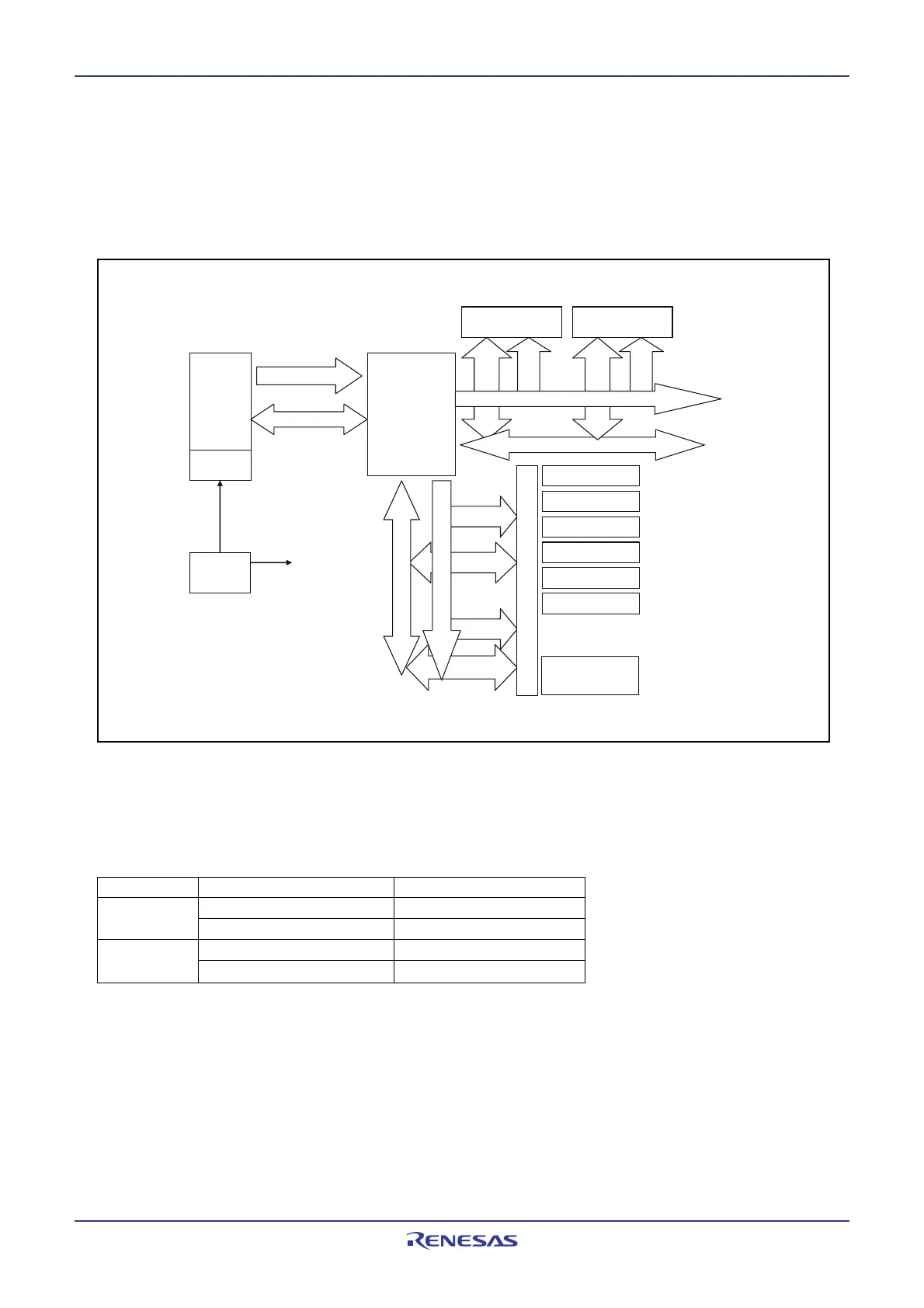
The internal bus consists of CPU bus, memory bus, and peripheral bus. Bus Interface Unit (BIU) is used to
interfere with CPU, ROM/RAM, and perpheral functions by controling CPU bus, memory bus, and periph-
eral bus. Figure 6.3 shows the block diagram of the internal bus.
CPU
ROM
BIU
I/O
CP
U address bus
Memory data bus
Periphral data bus
DMAC
Memory address bus
Peripheral address bus
Timer
WDT
Serial I/O
ADC
CAN
CRC
Peripheral function
CPU clock
RAM
CPU data bus
Peripheral function
.
.
Clock
generation
circuit
S F R
Figure 6.3 Bus Block Diagram
Table 6.1 Accessible Area and Bus Cycle
The number of bus cycle varies by the internal bus. Table 6.1 lists the accessible area and bus cycle.
Accessible Area Bus Cycle
SFR PM20 bit = 0 (2 waits) 3 CPU clock cycles
PM20 bit = 1 (1 wait) 2 CPU clock cycles
ROM/RAM PM17 bit = 0 (no wait) 1 CPU clock cycle
PM17 bit = 1 (1 wait) 2 CPU clock cycles
 Loading...


