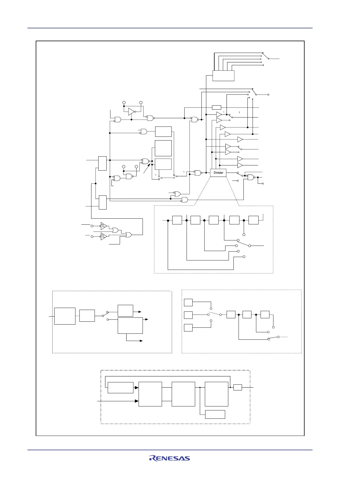
7. Clock Generation Circuit
page 48
854fo7002,03.raM21.1.veR
2110-1010B90JER
puorG92/C61M
Figure 7.1 Clock Generation Circuit
Phase
comparator
Charge
pump
Voltage
control
oscillator
(VCO)
PLL clock
Main clock
1/2
Programmable
counter
Internal low-
pass filter
PLL frequency synthesizer
Pulse generation
circuit for clock
edge detection
and charge,
discharge control
Charge,
discharge
circuit
Reset
generating
circuit
Oscillation stop,
re-oscillation
detection interrupt
generating circuit
Main
clock
Oscillation stop
detection reset
CM27=0
CM21 switch signal
Oscillation stop,
re-oscillation
detection signal
Oscillation stop, re-oscillation detection circuit
CM27=1
1/2 1/2 1/2
ROCR3, ROCR2=11
2
On-chip
oscillator
clock
1/8
1/4
1/2
ROCR3, ROCR2=10
2
ROCR3, ROCR2=01
2
ROCR1, ROCR0=00
2
f
1(ROC)
f
2(ROC)
f
3(ROC)
ROCR1,ROCR0=01
2
ROCR1, ROCR0=11
2
Variable On-chip Oscillator
Variable
on-chip
oscillator
2
1/32
Main clock
generating circuit
f
C
CM02
CM04
CM10=1(stop mode)
Q
S
R
WAIT instruction
CM05
QS
R
NMI
Interrupt request level judgment output
RESET
Software reset
CPU clock
CM07
=
0
CM07
=
1
1/2 1/2 1/2 1/2
CM06=0
CM17, CM16=00
2
CM06=0
CM17, CM16=01
2
CM06=0
CM17, CM16=10
2
CM06=1
CM06=0
CM17, CM16=11
2
d
a
Details of divider
Sub-clock
generating circuit
X
CIN
X
COUT
X
OUT
X
IN
b
1/2
c
f
32SIO
I
f
AD
e
1/2 1/4 1/8 1/16
1/32
P
LK
=
PLL
frequency
s
nt
es
z
r
M21=
M11
M21=
Sub-clock
On-chip
oscillator
clock
P
LK
=
1
I
P
LK1=1
P
LK1=
2
I
Main
clock
Oscillation
stop, re-
oscillation
detection
circuit
D4INT clock
BCLK
CLKOUT
I/O ports
PCLK5=0,CM01-CM00=00
2
PCLK5=0,CM01-CM00=012
PCLK5=1,
CM01-CM00=002
PCLK5=0,
CM01-CM00=10
2
PCLK5=0,
CM01-CM00=11
2
CAN module
system clock
divider
fCAN
CCLK2-CCLK0=0002
CCLK2-CCLK0=0012
CCLK2-CCLK0=0102
CCLK2-CCLK0=0112
CCLK2-CCLK0=1002
CM00, CM01, CM02, CM04, CM05, CM06, CM07: Bits in the CM0 register
CM10, CM11, CM16, CM17: Bits in the CM1 register
PCLK0, PCLK1, PCLK5: Bits in the PCLKR register
CM21, CM27: Bits in the CM2 register
CM21
 Loading...


