7. Clock Generation Circuit
page 50
854fo7002,03.raM21.1.veR
2110-1010B90JER
puorG92/C61M
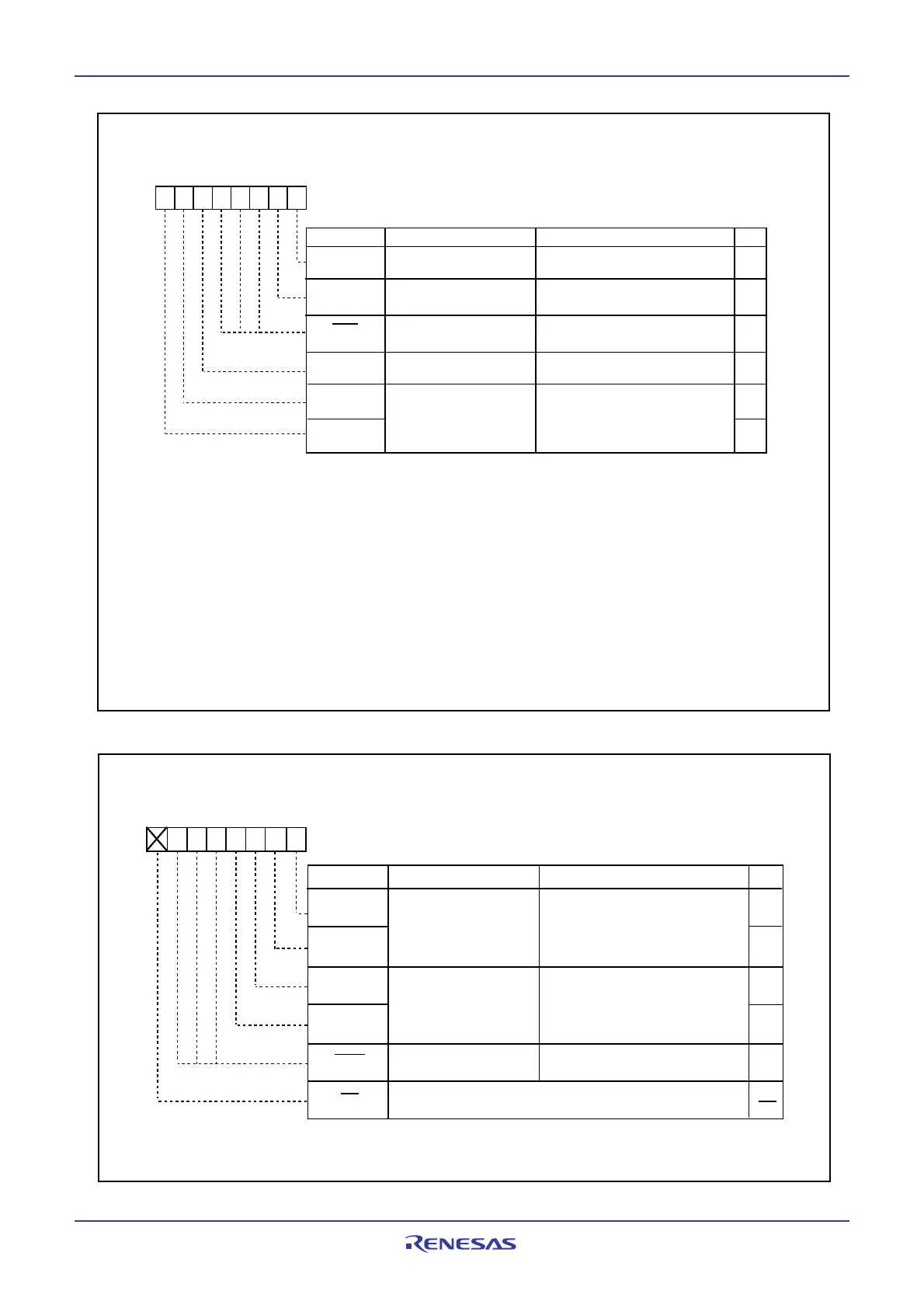
Figure 7.3 CM1 Register
Figure 7.4 ROCR Register
b7 b6 b5 b4 b3 b2 b1 b0
RW
ROCR0
ROCR1
On-chip Oscillator Control Register
(1)
Symbol Address After Reset
ROCR
025C
16
X00001012
Bit Name
Function
Bit Symbol
Frequency select bits
RW
RW
Reserved bit
000
0 0: f1 (ROC)
0 1: f
2 (ROC)
1 0: Do not set to this value
1 1: f
3 (ROC)
b1 b0
ROCR2
ROCR3
Divider select bits
RW
RW
0 0: Do not set to this value
0 1: divide by 2
1 0: divide by 4
1 1: divide by 8
b3 b2
NOTE:
1. Write to this register after setting the PRC0 bit in the PRCR register to 1 (write enable).
(b6-b4)
Set to 0
Nothing is assigned. When write, set to 0. When read, its
content is undefined
(b7)
RW
System Clock Control Register 1
(1)
Symbol Address After Reset
CM1 0007
16 001000002
Bit Name FunctionBit Symbol
b7 b6 b5 b4 b3 b2 b1 b0
CM10
All clock stop control bit
(4, 6)
0 : Clock on
1 : All clocks off (stop mode)
CM15
X
IN
-X
OUT
drive capacity
select bit
(2)
0 : LOW
1 : HIG
H
RW
CM16
CM17
Reserved bit
Set to
0
Main clock division
select bits
(3)
0 0 : No division mode
0 1 : Division by 2 mode
1 0 : Division by 4 mode
1 1 : Division by 16 mode
b7 b6
000
CM11
System clock select bit 1
(6, 7)
0 : Main clock
1 : PLL clock
(5)
RW
RW
RW
RW
RW
RW
(b4-b2)
NOTES:
1. Write to this register after setting the PRC0 bit in the PRCR register to 1 (write enable).
2. When entering stop mode from high or middle speed mode, or when the CM05 bit is set to 1 (main clock
turned off) in low speed mode, the CM15 bit is set to 1 (drive capability high).
3. Effective when the CM06 bit is 0 (bits CM16 and CM17 enable).
4. If the CM10 bit is 1 (stop mode), X
OUT
goes “H” and the internal feedback resistor is disconnected. The X
CIN
and X
COUT
pins are placed in the high-impedance state. When the CM11 bit is set to 1 (PLL clock), or the
CM20 bit in the CM2 register is set to 1 (oscillation stop, re-oscillation detection function enabled), do not set
the CM10 bit to 1.
5. After setting the PLC07 bit in the PLC0 register to 1 (PLL operation), wait until tsu (PLL) elapses before setting
the CM11 bit to 1 (PLL clock).
6. When the PM21 bit in the PM2 register is set to 1 (clock modification disable), writing to bits CM10, CM11 has
no effect. When the PM22 bit in the PM2 register is set to 1 (watchdog timer count source is on-chip oscillator
clock), writing to the CM10 bit has no effect.
7. Effective when CM07 bit is 0 and CM21 bit is 0 .
 Loading...


