7. Clock Generation Circuit
page 52
854fo7002,03.raM21.1.veR
2110-1010B90JER
puorG92/C61M
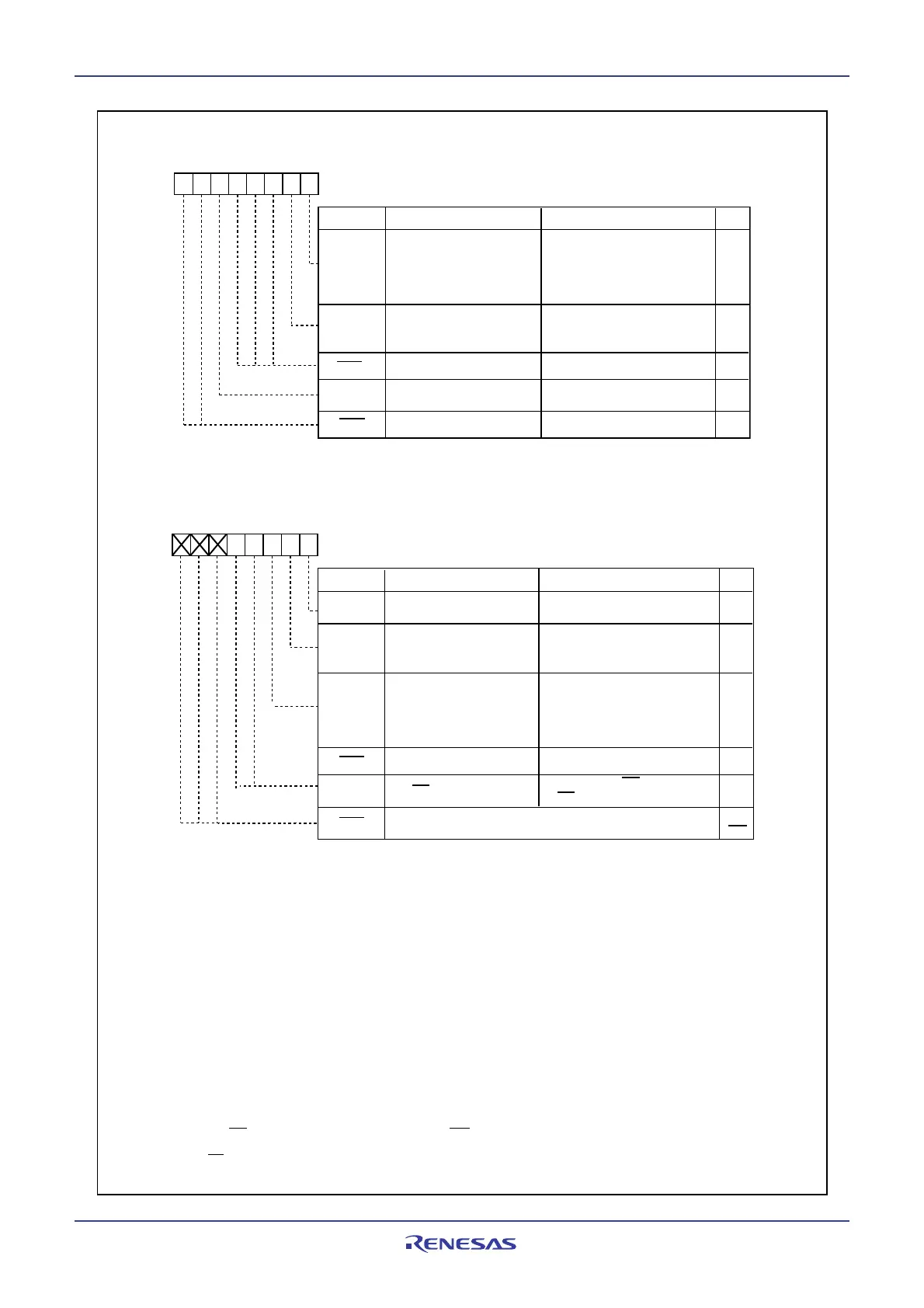
Figure 7.6 PCLKR Register and PM2 Register
NOTES:
1. Write to this register after setting the PRC1 bit in the PRCR register to 1 (write enable).
2. The PM20 bit becomes effective when PLC07 bit in the PLC0 register is set to 1 (PLL on). Change the PM20
bit when the PLC07 bit is set to 0 (PLL off). Set the PM20 bit to 0 (2 waits) when PLL clock > 16MHz.
3. Once this bit is set to 1, it cannot be cleared to 0 by program.
4. Writting to the following bits has no effect when the PM21 bit is set to 1:
CM02 bit in the CM0 register
CM05 bit in the CM0 register (main clock is not halted)
CM07 bit in the CM0 register (CPU clock source does not change)
CM10 bit in the CM1 register (stop mode is not entered)
CM11 bit in the CM1 register (CPU clock source does not change)
CM20 bit in the CM2 register (oscillation stop, re-oscillation detection function settings do not change)
All bits in the PLC0 register (PLL frequency synthesizer setting do not change)
Do not execute WAIT instruction when the PM21 bit is set to 1.
5. Setting the PM22 bit to 1 results in the following conditions:
•
The on-chip oscillator continues oscillating even if the CM21 bit in the CM2 register is set to "0" (main clock or
PLL clock) (system clock of count source selected by the CM21 bit is valid)
• The on-chip oscillator starts oscillating, and the on-chip oscillator clock becomes the watchdog timer
count source.
• The CM10 bit in the CM1 register cannnot be written. (Writing 1 has no effect, stop mode is not entered.)
• The watchdog timer does not stop in wait mode.
6. For NMI function, the PM24 bit must be set to 1(NMI function). Once this bit is set to 1, it cannot be set to 0 by
program.
7. SD input is valid regardless of the PM24 setting.
Function
Bit Symbol
Bit Name
Processeor Mode Register 2
(1)
Symbol Address After Reset
PM2 001E
16
XXX00000
2
RW
b7 b6 b5 b4 b3 b2 b1 b0
PM20
0
PM21
RW
RW
RW
(b7-b5)
PM22
PM24
(b3)
Reserved bit Set to 0
RW
RW
Nothing is assigned. When write, set to 0.
When read, thecontent is undefined
0: CPU clock is used for the
watchdog timer count source
1: On-chip oscillator clock is used
for the watchdog timer count
source
0: 2 waits
1: 1 wait
Specifying wait when
accessing SFR
(2)
System clock protective
bit
(3,4)
WDT count source
protective bit
(3,5)
0: Clock is protected by PRCR
register
1: Clock modification disabled
P8
5/NMI configuration bit(6,7)
0: P8
5
function (NMI disabled)
1: NMI function
Function
Bit Symbol
Bit Name
Peripheral Clock Select Register
(1)
Symbol
Address
After Reset
PCLKR 025E
16
00000011
2
RW
b7 b6 b5 b4 b3 b2 b1 b0
PCLK0
0: f
2
1: f
1
000
Reserved bit Set to 0
NOTE:
1. Write to this register after setting the PRC0 bit in PRCR register to 1 (write enable).
00
PCLK1
0: f
2
SIO
1: f
1
SIO
RW
RW
RW
(b4-b2)
Reserved bit
Set to 0 RW
(b7-b6)
RW
PCLK5
Refer to Table 7.3
Clock output function
expansion select bit
Timers A, B clock select bit
(Clock source for the timers A,
B, the timer S, the dead timer,
SI/O3, SI/O4 and multi-master
I
2
C bus)
SI/O clock select bit
(Clock source for UART0 to
UART2)
 Loading...


