7. Clock Generation Circuit
page 53
854fo7002,03.raM21.1.veR
2110-1010B90JER
puorG92/C61M
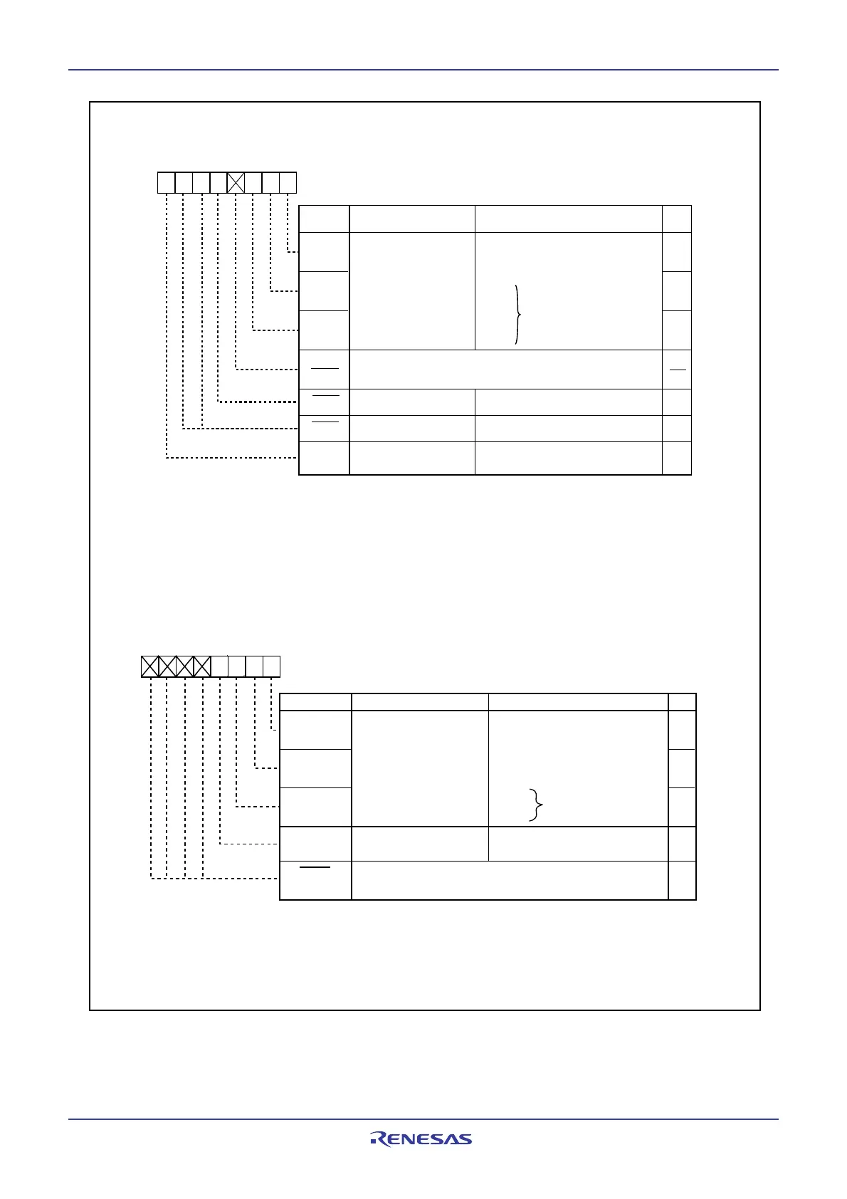
Figure 7.7 PLC0 Register and CCLKR register
PLC00
PLC01
PLC02
PLC07
(3)
(4)
Function
NOTES:
1. Write to this register after setting the PRC0 bit in the PRCR register to 1 (write enable).
2. When the PM21 bit in the PM2 register is 1 (clock modification disable), writing to this register has no effect.
3.
These three bits can only be modified when the PLC07 bit is set to 0 (PLL turned off). The value once written to
this bit cannot be modified.
4. Before setting this bit to 1 , set the CM07 bit to 0 (main clock), set bits CM17 to CM16 bits to 002 (main
clock undivided mode), and set the CM06 bit to 0 (CM16 and CM17 bits enable).
PLL Control Register 0
(1,2)
PLL multiplying factor
select bit
Nothing is assigned. If necessary, set to 0.
When read, the content is undefined
Operation enable bit
0 0 0:
0 0 1: Multiply by 2
0 1 0: Multiply by 4
0 1 1:
1 0 0:
1 0 1:
1 1 0:
1 1 1:
0: PLL Off
1: PLL On
Bit Name
Bit
Symbol
Symbol Address After Reset
PLC0 001C
16 0001X0102
RW
b1b0b2
Reserved bit Set to 0
Do not set
RW
RW
RW
RW
RW
Reserved bit Set to 1 RW
Do not set
(b4)
(b6-b5)
(b3)
b7 b6 b5 b4 b3 b2 b1 b0
0 10
RW
RW
RW
RW
RW
0 0 0 No division
0 0 1: Divide-by-2
0 1 0: Divide-by-4
0 1 1: Divide-by-8
1 0 0: Divide-by-16
1 0 1:
1 1 0: Inhibited
1 1 1:
b2 b1 b0
CAN0 clock select bits
(2)
CAN0 CPU interface
sleep bit
(3)
0: CAN0 CPU interface operating
1: CAN0 CPU interface in sleep
Bit Name FunctionBit Symbol
RW
CCLK3
CCLK1
CCLK2
CCLK0
Symbol Address After Reset
CCLKR 025F16 0016
NOTES:
1. Write to this register after setting the PRC0 bit in the PRCR register to 1 (write enable).
2. Configuration of bits CCLK2 to CCLK0 can be done only when the Reset bit in the C0CTLR register is set to 1
(Reset/Initialization mode).
3. Before setting this bit to 1(CAN0 CPU interface in sleep), set the Sleep bit in C0CTLR register to 1 (Sleep
mode).
CAN0 Clock Select Register
(1)
b7 b6 b5 b4 b3 b2 b1 b0
(b7-b4)
Nothing is assigned. If necessary, set to 0. When read,
the content is 0
 Loading...


