UART0 to UART2
M30240 Group
Rev.1.00 Sep 24, 2003 Page 90 of 360
1.2.23.1.4 Continuous receive mode
If the continuous receive mode enable bit (bits 2 and 3 at address 03B0
16
, bit 5 at address 037D
16
) is set to
“1”, the unit is placed in continuous receive mode. In this mode, when the receive buffer register is read out,
the unit simultaneously goes to a receive enable state without having to set dummy data to the transmit buffer
register back again.
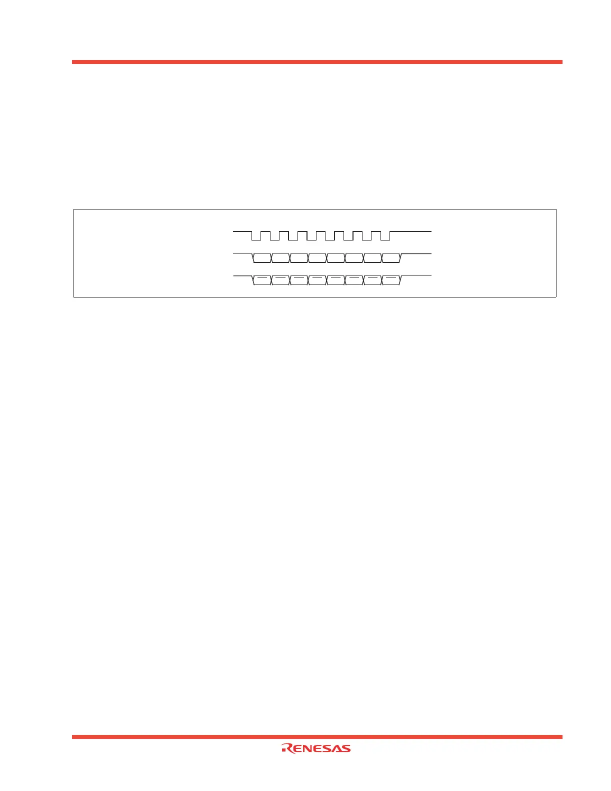
1.2.23.1.5 Serial data logic switch function (UART2)
When the data logic select bit (bit6 at address 037D
16
) = “1”, and writing to transmit buffer register or reading
from receive buffer register, data is reversed. Figure 1.86 shows the example of serial data logic switch timing.
Figure 1.86: Serial data logic switch timing
D0 D1 D2 D3 D4 D5 D6 D7
D0 D1 D2 D3 D4 D5 D6 D7
Transfer clock
TxD
2
(no reverse)
TxD
2
(reverse)
“H”
“L”
“H”
“L”
“H”
“L”
•When LSB first
 Loading...


