UART0 to UART2
M30240 Group
Rev.1.00 Sep 24, 2003 Page 97 of 360
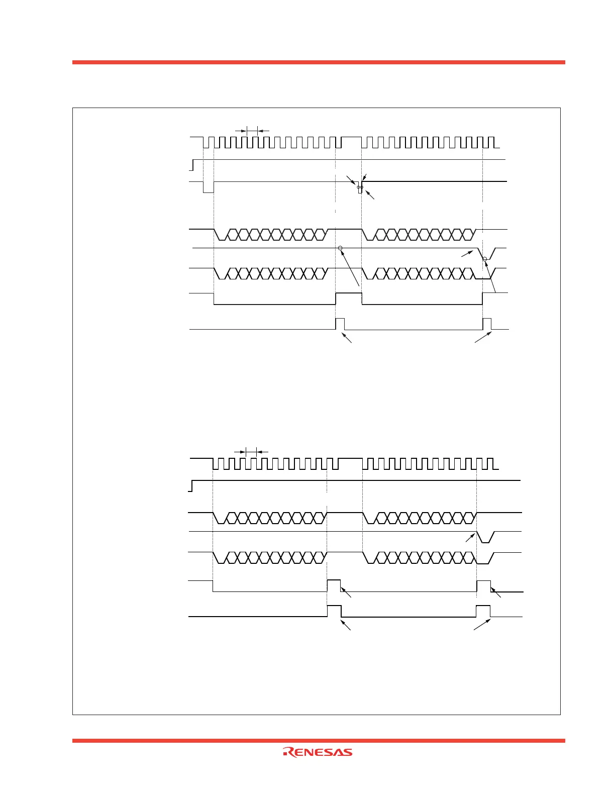
Figure 1.92: Typical transmit/receive timing in UART mode (compliant with the SIM interface)
Transmit enable
bit(TE)
Transmit buffer
empty flag(TI)
Transmit register
empty flag (TXEPT)
D0
D1 D2
D3
D4 D5
D6
D7ST
P
Start
bit
Parity
bit
The above timing applies to the following settings :
• Parity is enabled.
• One stop bit.
• Transmit interrupt cause select bit = “1”.
“0”
“1”
“0”
“1”
“0”
“1”
Tc = 16 (n + 1) / fi
fi : frequency of BRG2 count source (f
1
, f
8
, f
32
)
n : value set to BRG2
Transmit interrupt
request bit (IR)
“0”
“1”
D0 D1 D2
D3
D4
D5 D6
D7ST
P
Shown in ( ) are bit symbols.
Tc
Transfer clock
SP
Stop
bit
Data is set in UART2 transmit buffer register
SP
A “L” level returns from TxD
2
due to
the occurrence of a parity error.
The level is detected by the
interrupt routine.
The level is
detected by the
interrupt routine.
Receive enable
bit (RE)
Receive complete
flag (RI)
D0
D1 D2
D3
D4 D5 D6
D7
ST
P
Start
bit
Parity
bit
RxD2
The above timing applies to the following settings :
• Parity is enabled.
• One stop bit.
• Transmit interrupt cause select bit = “0”.
“0”
“1”
“0”
“1”
Tc = 16 (n + 1) / fi
fi : frequency of BRG2 count source (f
1
, f
8
, f
32
)
n : value set to BRG2
Receive interrupt
request bit (IR)
“0”
“1”
D0
D1 D2
D3
D4 D5 D6
D7
ST
P
SP
Shown in ( ) are bit symbols.
Tc
Transfer clock
SP
Stop
bit
A “L” level returns from TxD
2
due to
the occurrence of a parity error.
TxD2
Read to receive buffer
Read to receive buffer
D0
D1 D2
D3
D4 D5 D6
D7
ST
P
Signal conductor level
(Note 2)
D0
D1 D2
D3
D4 D5 D6
D7
ST
P
SP
SP
D0
D1
D2 D3
D4 D5 D6
D7ST
P
D0
D1 D2
D3
D4 D5
D6
D7ST
P
SP
SP
TxD2
RxD2
Signal conductor level
(Note 2)
Transferred from UART2 transmit buffer register to UART2 transmit register
Cleared to “0” when interrupt request is accepted, or cleared by software
Cleared to “0” when interrupt request is accepted, or cleared by software
Note 1: The transmit is started with overflow timing of BRG after having written in a value at the transmit buffer in the above timing.
Note 1
Note 2: Equal in waveform because TxD2 and RxD2 are connected.
Note 2: Equal in waveform because TxD2 and RxD2 are connected.
 Loading...


