UART0 to UART2
M30240 Group
Rev.1.00 Sep 24, 2003 Page 98 of 360
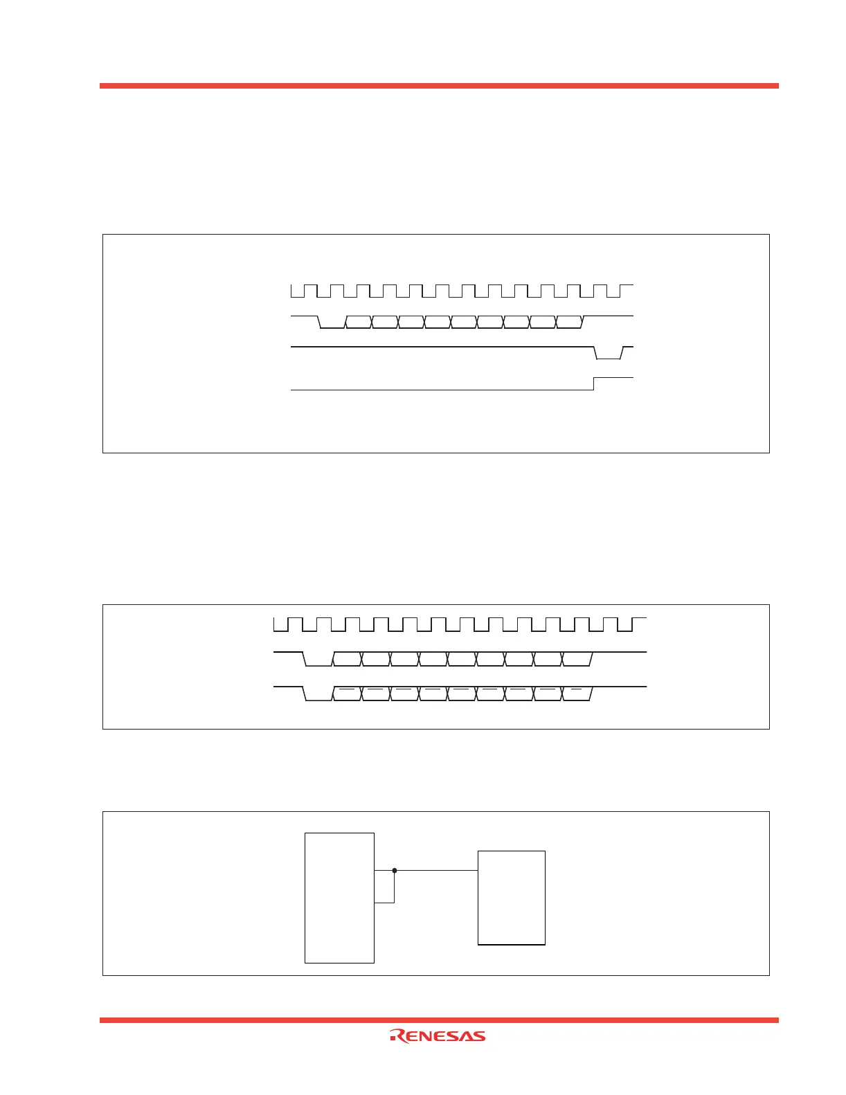
1.2.23.3.1 Function for outputting a parity error signal
With the error signal output enable bit (bit 7 of address 037D
16
) assigned “1”, you can output an “L” level from
the TxD2 pin when a parity error is detected. In step with this function, the generation timing of a transmission
completion interrupt changes to the detection timing of a parity error signal. Figure 1.93 shows the output tim-
ing of the parity error signal.
Figure 1.93: Output timing of the parity error signal
1.2.23.3.2 Direct format/inverse format
Connecting the SIM card allows you to switch between direct format and inverse format. If you choose the
direct format, D0 data is output from TxD2. If you choose the inverse format, D7 data is inverted and output
from TxD2.
Figure 1.94 shows the SIM interface format.
Figure 1.94: SIM interface format
Figure 1.95 shows the example of connecting the SIM interface with TxD2 and RxD2.
Figure 1.95: Connecting the SIM interface
ST : Start bit
P : Even Parity
D0 D1 D2 D3 D4 D5 D6 D7 P SPST
Hi-Z
Transfer
clock
RxD
2
TxD
2
Receive
complete flag
“H”
“L”
“H”
“L”
“H”
“L”
“1”
• LSB first
“0”
SP: Stop bit
P : Even parity
D0
D1 D2 D3 D4 D5 D6 D7 P
Transfer
clock
TxD
2
(direct)
TxD
2
(inverse)
D7 D6 D5 D4 D3 D2 D1 D0 P
Microcomputer
SIM card
TxD
2
RxD
2
 Loading...


