Electrical characteristics
M30240 Group
Rev.1.00 Sep 24, 2003 Page 127 of 360
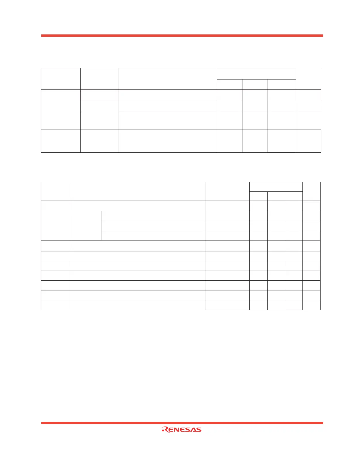
Table 1.40: USB Electrical Characteristics (Vcc=4.1~5.25V, Vss=0V, Ta= 0°C∼ 70°C, f(Xin) = 12MHz)
Note: See Fig. 1.120 for recommended configuration.
Symbol Parameter Measuring Condition
Standard
Unit
Min Typ Max
V
OH D+, D- I=18.3 mA, RX=33 Ω, VXcap =3.0 V 2.2 V
V
OL D+, D- I=18.3 mA, RX=33 Ω, VXcap =3.0 V 0.8 V
Isusp
Suspend
current
USB suspend mode, internal clock
stopped
175 µA
Xcap
DC-DC
converter
voltage
DC-DC converter output voltage on
Xcap pin
3.0 3.3 3.6 V
Table 1.41: A-D conversion characteristics (Vcc, Avcc = 4.1~5.25V, Vss=0V, Ta= 0°C~ 70°C, f(Xin) = 12MHz)
Symbol Parameter
Measuring
condition
Standard
Unit
Min Typ Max
- Resolution V
REF = Vcc 10 Bits
-
Absolute
accuracy
Sample and hold function not available V
REF = Vcc = 5V ±3 LSB
Sample and hold function available (10bit) VREF = Vcc = 5V ±3 LSB
Sample and hold function available (8bit) V
REF = Vcc = 5V ±2 LSB
R
LADDER
Ladder resistance VREF = Vcc = 5V 10 40 kΩ
t
CONV Conversion time (10bit) 2.75 µs
t
CONV Conversion time (8bit) 2.34 µs
tSAMP Sampling time 0.25 µs
V
REF Reference voltage 2 V
V
IA Analog input voltage (min. operating frequency =x) 0 VREF V
φAD A-D clock frequency 1 12 MHz
 Loading...


