Switching behavior Power to the input starts the assigned function, e.g. start read cycle.
Default setting in the device: logic not inverted (active high), debounce
time 10ms
Properties
•
Opto-decoupled, reverse polarity protected
•
Can be wired with PNP output of a trigger sensor
Electrical values Low: V
in
1)
≤2V; I
in
2)
≤0.3mA
High: 6V ≤V
in
≤27.6V; 0.7mA ≤I
in
≤5mA
1)
Input voltage.
2)
Input current.
NOTE
Assign the functions for the digital inputs in the device using a configuration software,
e.g., SOPASET.
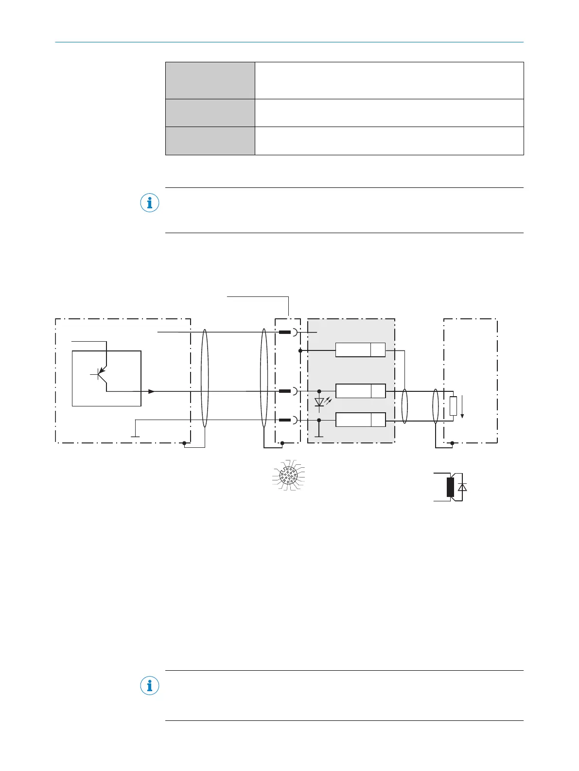
13.3.7 Wiring digital outputs of the device in the CDB650-204
Device = Lector61x = V2D61xx- xxxxxEx
22
GND
5Shield
D
RES/OUT C
3
1
7
2
6
5
4
8
13
14
17
15
9
10
12
16
11
7
Device 1
CDB650-204
Load (e.g. PLC) 4
1
.
.
.
U
IN
*V
S
GND
V
out
Result A
GND
B
2
2
5
For inductive load: 6
Cable 3
Figure 36: Wire the digital output in the CDB650-204 connection module.
1
Device
2
Supply voltage V
S
3
Connecting cable permanently connected with the device (male connector, M12, 17-pin, A-coded)
4
Load (e.g. PLC)
5
Output voltage V
out
6
With inductive load: see note
7
Connection module: female connector, M12, 17-pin, A-coded
Inductive load
NOTE
Provide an arc-suppression switch at the digital output if inductive load is present.
►
Attach a freewheeling diode directly to the load for this purpose.
ANNEX 13
8024830/1MBT/2024-05-22 | SICK O P E R A T I N G I N S T R U C T I O N S | Lector61x
69
Subject to change without notice