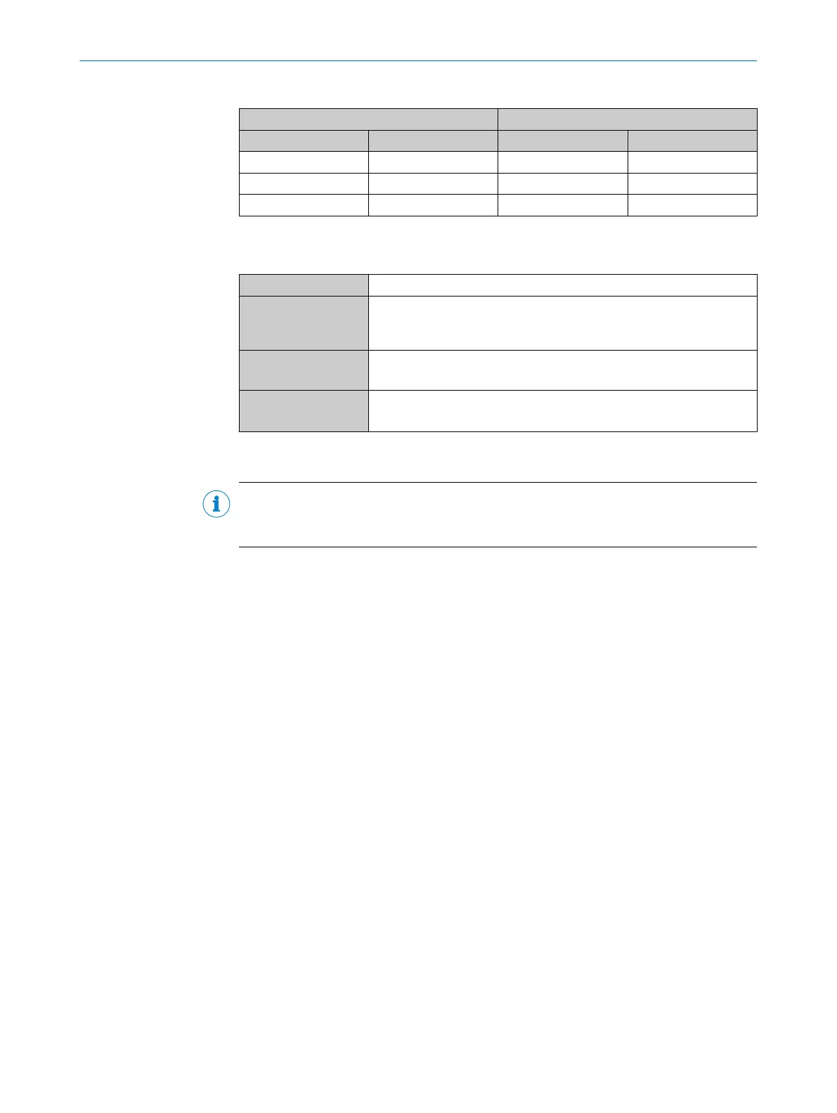
Table 25: Assignment of placeholders to the digital outputs
Device CDB650-204
Output A Pin B Signal C Terminal D
Result 1 13 RES/OUT 1 20
Result 2 14 RES/OUT 2 21
Result 3 16 RES/OUT 3 50
Characteristic data of the digital outputs
Table 26: Characteristic data of the digital switching outputs
Type Switching
Switching behavior PNP switching to supply voltage V
S
Default settings in the device: no function, logic: not inverted (active
high)
Properties
•
Short-circuit protected and temperature protected
•
Not electrically isolated from V
S
Electrical values 0V ≤V
out
1)
≤V
S
(V
S
−1.5V) ≤ V
out
≤ V
S
at I
out
2)
≤50mA
1)
Output voltage.
2)
Output current.
NOTE
Allocate the functions for the digital outputs in the device using a configuration soft‐
ware, e.g., SOPASET.
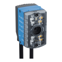
13.4 Connection diagrams of connection module CDM420-0006
13.4.1 Connection of the device to CDM420-0006
Device = Lector61x = V2D61xx-xxxxxEx
13 ANNEX
70
O P E R A T I N G I N S T R U C T I O N S | Lector61x 8024830/1MBT/2024-05-22 | SICK
Subject to change without notice