EasyManua.ls Logo

ST STM32F0 Series User Manual

ST STM32F0 Series
91 pages
To Next Page IconTo Next Page
To Previous Page IconTo Previous Page
Page #13 background imageLoading...
Page #13 background image
PM0215 The STM32 Cortex-M0 processor
Doc ID 022979 Rev 1 13/91
Stack pointer (SP) register R13
In Thread mode, bit[1] of the CONTROL register indicates the stack pointer to use:
0: Main Stack Pointer (MSP)(reset value). On reset, the processor loads the MSP with
the value from address 0x00000000.
1: Process Stack Pointer (PSP).
Link register (LR) register R14
Stores return information for subroutines, function calls, and exceptions. On reset, the
processor loads the LR value 0xFFFFFFFF.
Program counter (PC) register R15
Contains the current program address. On reset, the processor loads the PC with the value
of the reset vector, which is at address 0x00000004. Bit[0] of the value is loaded into the
EPSR T-bit at reset and must be 1.
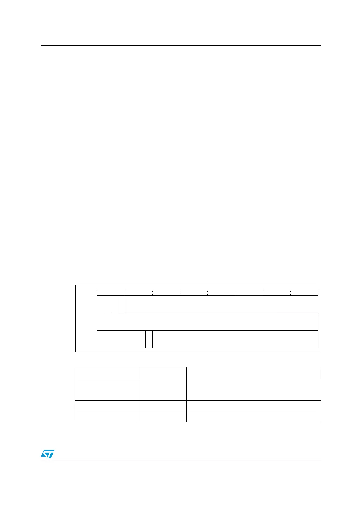
Program status register
The Program Status Register (PSR) combines:
Application program status register (APSR)
Interrupt program status register (IPSR)
Execution program status register (EPSR)
These registers are mutually exclusive bitfields in the 32-bit PSR. They can be accessed
individually or as a combination of any two or all three registers, using the register name as
an argument to the MSR or MRS instructions. For example:
Read all of the registers using PSR with the MRS instruction
Write to the APSR using APSR with the MSR instruction.
Figure 3. APSR, IPSR and EPSR bit assignments
Table 4. PSR register combinations and attributes
Register Type Combination
PSR read-write
(1), (2)
1. The processor ignores writes to the IPSR bits.
2. Reads of the EPSR bits return zero, and the processor ignores writes to the these bits
APSR, EPSR, and IPSR
IEPSR read-only EPSR and IPSR
IAPSR read-write
(1)
APSR and IPSR
EAPSR read-write
(2)
APSR and EPSR
  
5HVHUYHG ([FHSWLRQQXPEHU
    
1=&9
5HVHUYHG
$365
,365
(365
5HVHUYHG 5HVHUYHG7

Table of Contents

Other manuals for ST STM32F0 Series

Question and Answer IconNeed help?

Do you have a question about the ST STM32F0 Series and is the answer not in the manual?

ST STM32F0 Series Specifications

General IconGeneral
SeriesSTM32F0
CoreARM Cortex-M0
Operating FrequencyUp to 48 MHz
Flash Memory16 KB to 256 KB
SRAM4 KB to 32 KB
ADC Resolution12-bit
ADC ChannelsUp to 16
Operating Voltage2.0 V to 3.6 V
DAC Resolution12-bit (some series)
Communication InterfacesI2C, SPI, USART, USB, CAN
Operating Temperature-40°C to 85°C
Package OptionsLQFP, TSSOP, UFQFPN, WLCSP

Summary

Introduction to STM32F0xxx Programming

About this document

1.1 Typographical conventions

Defines typographical conventions used in the document.

1.2 List of abbreviations for registers

Lists abbreviations used for register descriptions.

1.3 About the STM32 Cortex-M0 processor and core peripherals

Overview of the Cortex-M0 processor and its core peripherals.

The STM32 Cortex-M0 processor

2.1 Programmers model

Describes the Cortex-M0 programmer's model, modes, and stacks.

2.2 Memory model

Details the processor memory map and memory access behavior.

2.3 Exception model

Explains the exception model, states, types, and priorities.

2.4 Fault handling

Covers fault handling mechanisms, including lockup states.

2.5 Power management

Describes sleep and deep sleep modes for power saving.

The STM32 Cortex-M0 instruction set

3.1 Instruction set summary

Summarizes the Thumb instruction set supported by the Cortex-M0.

3.4 Memory access instructions

Covers instructions for loading and storing data from/to memory.

3.5 General data processing instructions

Describes instructions for arithmetic, logical, and data manipulation operations.

3.6 Branch and control instructions

Details instructions for program flow control and branching.

Core peripherals

4.1 About the STM32 Cortex-M0 core peripherals

Introduces the core peripherals and their address map.

4.2 Nested vectored interrupt controller (NVIC)

Details the NVIC's support for interrupts and its registers.

4.3 System control block (SCB)

Describes the SCB for system implementation information and control.

4.4 SysTick timer (STK)

Explains the SysTick timer's functionality and registers.

Revision history

Related product manuals