EasyManua.ls Logo

ST STM32F0 Series User Manual

ST STM32F0 Series
91 pages
To Next Page IconTo Next Page
To Previous Page IconTo Previous Page
Page #80 background image
Core peripherals PM0215
80/91 Doc ID 022979 Rev 1
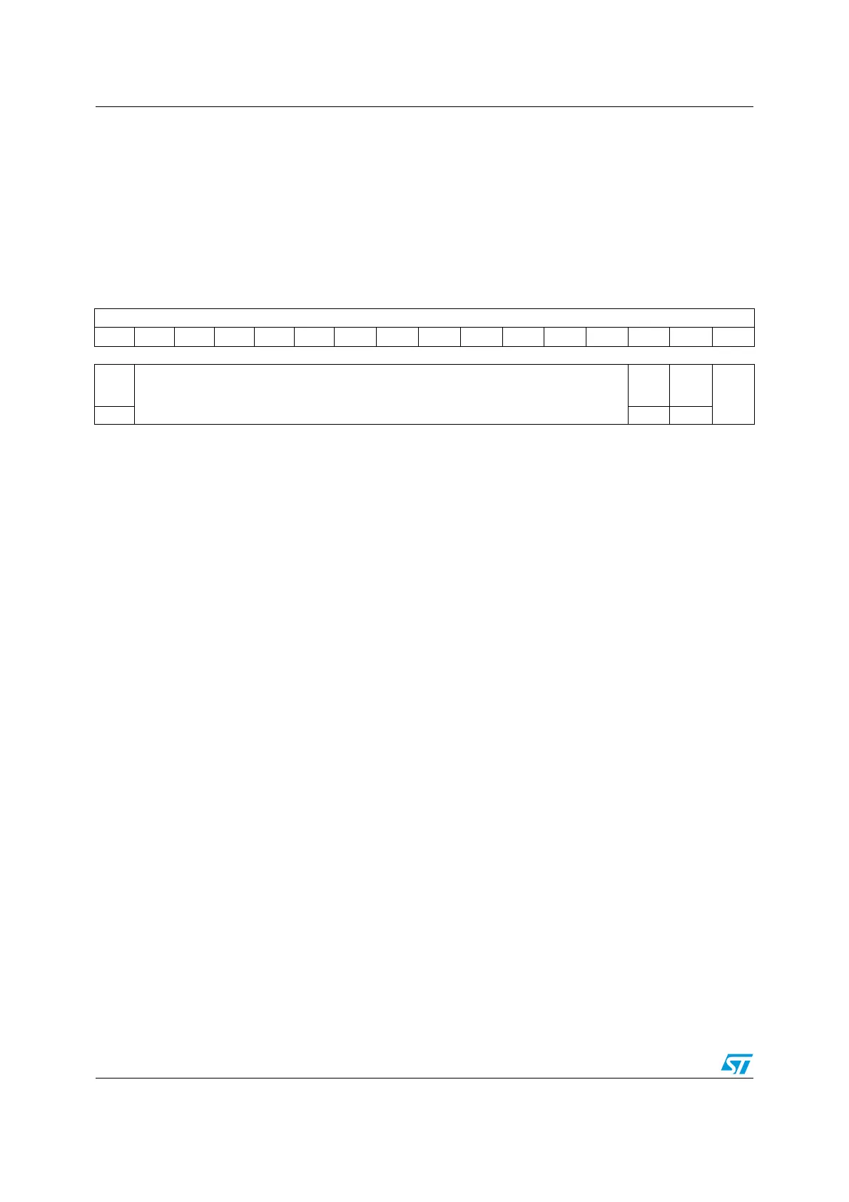
4.3.3 Application interrupt and reset control register (AIRCR)
Address offset: 0x0C
Reset value: 0xFA05 0000
The AIRCR provides endian status for data accesses and reset control of the system.
To write to this register, you must write 0x5FA to the VECTKEY field, otherwise the
processor ignores the write.
31 30 29 28 27 26 25 24 23 22 21 20 19 18 17 16
Reserved(read)/ VECTKEY[15:0](write)
rw rw rw rw rw rw rw rw rw rw rw rw rw rw rw rw
1514131211109876543210
ENDIA
NESS
Reserved
SYS
RESET
REQ
VECT
CLR
ACTIVE
Reserv
ed
r ww
Bits 31:16 Reserved / VECTKEY Register key
Reads as unknown
On writes, write 0x5FA to VECTKEY, otherwise the write is ignored.
Bit 15 ENDIANESS Data endianness bit
Reads as 0.
0: Little-endian
Bits 14:3 Reserved, must be kept cleared
Bit 2 SYSRESETREQ System reset request
Reads as 0.
0: No system reset request
1: Asserts a signal to the outer system that requests a reset.
Bit 1 VECTCLRACTIVE
Reserved for Debug use. This bit reads as 0. When writing to the register you must write 0 to
this bit, otherwise behavior is unpredictable.
Bit 0 Reserved, must be kept cleared

Table of Contents

Other manuals for ST STM32F0 Series

Question and Answer IconNeed help?

Do you have a question about the ST STM32F0 Series and is the answer not in the manual?

ST STM32F0 Series Specifications

General IconGeneral
SeriesSTM32F0
CoreARM Cortex-M0
Operating FrequencyUp to 48 MHz
Flash Memory16 KB to 256 KB
SRAM4 KB to 32 KB
ADC Resolution12-bit
ADC ChannelsUp to 16
Operating Voltage2.0 V to 3.6 V
DAC Resolution12-bit (some series)
Communication InterfacesI2C, SPI, USART, USB, CAN
Operating Temperature-40°C to 85°C
Package OptionsLQFP, TSSOP, UFQFPN, WLCSP

Summary

Introduction to STM32F0xxx Programming

About this document

1.1 Typographical conventions

Defines typographical conventions used in the document.

1.2 List of abbreviations for registers

Lists abbreviations used for register descriptions.

1.3 About the STM32 Cortex-M0 processor and core peripherals

Overview of the Cortex-M0 processor and its core peripherals.

The STM32 Cortex-M0 processor

2.1 Programmers model

Describes the Cortex-M0 programmer's model, modes, and stacks.

2.2 Memory model

Details the processor memory map and memory access behavior.

2.3 Exception model

Explains the exception model, states, types, and priorities.

2.4 Fault handling

Covers fault handling mechanisms, including lockup states.

2.5 Power management

Describes sleep and deep sleep modes for power saving.

The STM32 Cortex-M0 instruction set

3.1 Instruction set summary

Summarizes the Thumb instruction set supported by the Cortex-M0.

3.4 Memory access instructions

Covers instructions for loading and storing data from/to memory.

3.5 General data processing instructions

Describes instructions for arithmetic, logical, and data manipulation operations.

3.6 Branch and control instructions

Details instructions for program flow control and branching.

Core peripherals

4.1 About the STM32 Cortex-M0 core peripherals

Introduces the core peripherals and their address map.

4.2 Nested vectored interrupt controller (NVIC)

Details the NVIC's support for interrupts and its registers.

4.3 System control block (SCB)

Describes the SCB for system implementation information and control.

4.4 SysTick timer (STK)

Explains the SysTick timer's functionality and registers.

Revision history

Related product manuals